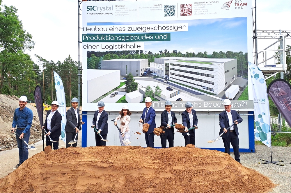
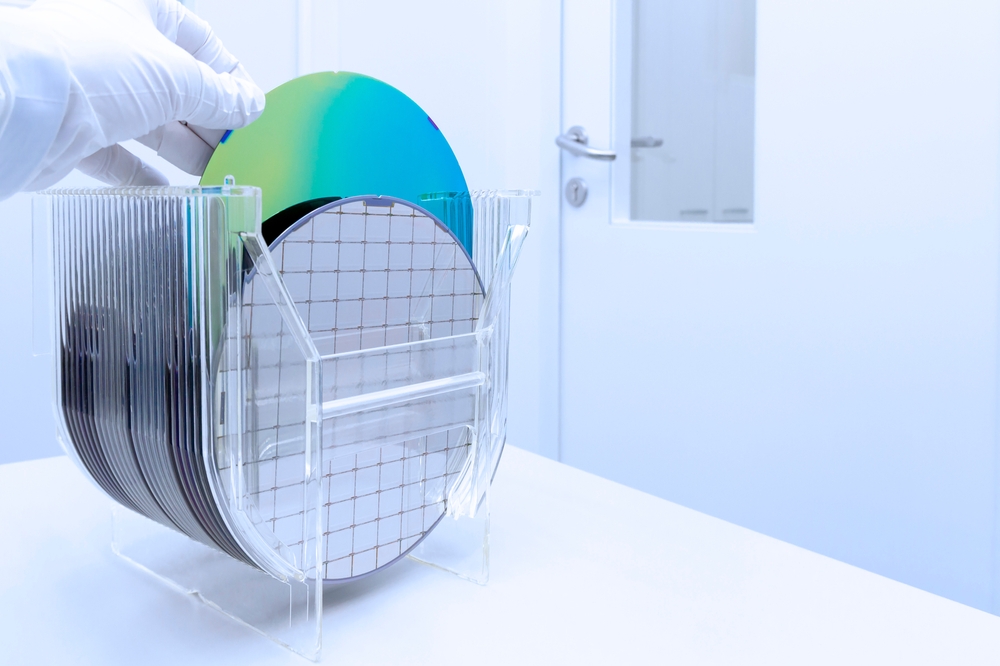
J2 to build Hong Kong's first 8-inch SiC fab

Company plans to start volume production in the next couple of years
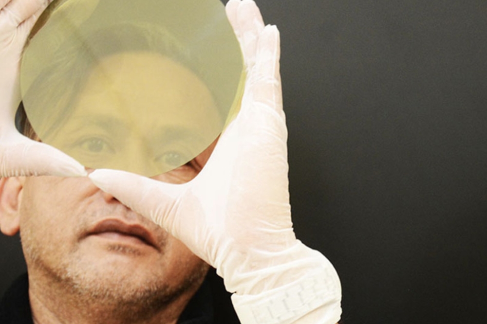
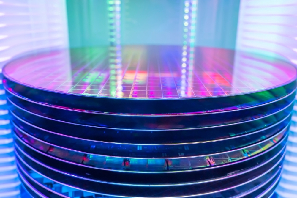
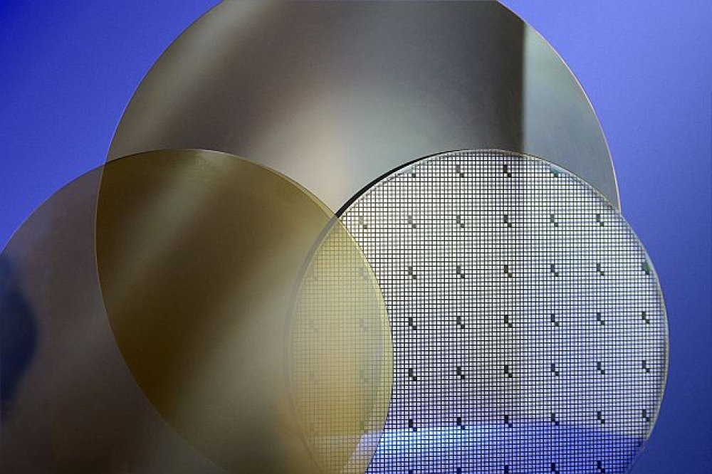
The Hong Kong Science and Technology Parks Corporation (HKSTP) has signed an agreement with mainland China-based J2 Semiconductor to set up an R&D Centre at the Hong Kong Science Park, and Hong Kong's first SiC 8-inch wafer fab.
J2 Semiconductor will invest an estimated $900 million (HK$6.9 billion) into the project, with plans to start volume production in the next couple of years. It expects to reach annual production capacity of 240,000 SiC wafers in 2028, and create more than 700 job positions in Hong Kong.
Sunny Chai, chairman of HKSTP said, "The plan of establishing J2 Semiconductor's R&D Centre in the Science Park will promote Hong Kong's R&D and advanced manufacturing capabilities of third-generation semiconductor devices. J2 Semiconductor brings the core technology and expertise to Hong Kong in advanced chip design, fabrication process and semiconductor product development. "
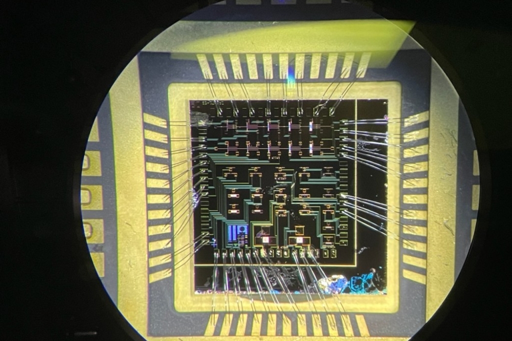
J2 Semiconductor mainly provides SiC devices with a focus on automotive, power conversion and communications.