Trimming the on-resistance of GaN MOSFETs
Nitrogen radical treatment, followed by insertion of an AlN interlayer, increases channel mobility in GaN MOSFETs
A team from Japan has reduced the on-resistance of its GaN MOSFETs by a factor of four through the introduction of a nitrided interface.
This advance by engineers from Toyoda Central Labs and the Institute of Materials Systems for Sustainability will help the development of devices that handle high voltages and currents at high efficiencies, a necessity for high-efficiency power conversion systems.
Potential candidates for such systems are a number of vertical device structures, including several forms of JFET. But these devices are held back by a limited gate overdrive, says team spokesman Kenji Ito, who points out that when the gate voltage exceeds 3 V the gate leakage current climbs, due to the forward current of the gate p-n diode. To suppress this leakage, there’s a need to limit the applied gate voltage – and thus prohibit the use of gate overdrive.
In stark contrast, MOSFETs have an extremely low gate-leakage current, thanks to the oxide/semiconductor junction that forms the gate structure.
One issue with GaN MOSFETs is that for a channel mobility of 100 cm2 V-1 s-1, channel resistance is 0.5 mΩ cm2, a concern at 1 kV or more. Another weakness is insufficient reliability of the gate oxide.
Ito and co-workers are tackling both these issues. Back in 2020 they revealed that the introduction of an AlSiO gate oxide enabled a lifetime of 20 years under 5 MV cm-1 at 150 °C. However, the channel mobility was no better than 40 cm2 V-1 s-1. Now, thanks to nitridation, they have overcome that limitation, with mobility reaching 200 cm2 V-1 s-1.
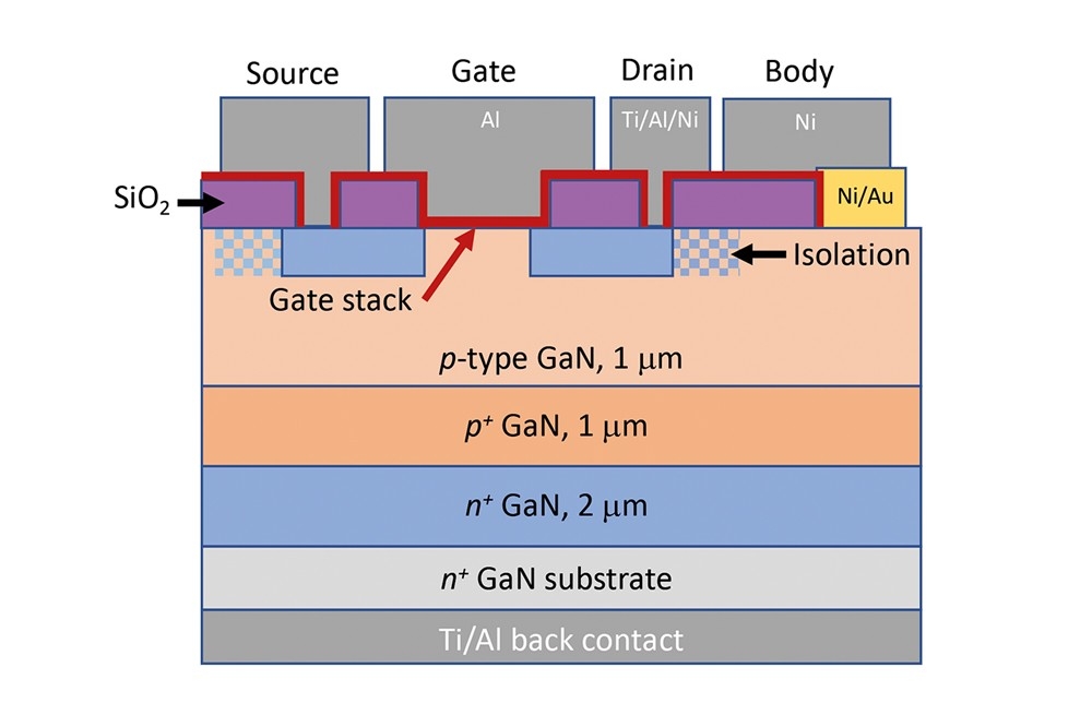
Fabrication of these transistors began by loading n-type GaN substrates into an MOCVD chamber and depositing a stack of epilayers. Post-growth annealing at 850 °C activated the magnesium acceptors. Silicon-ion implantation and annealing created source and drain regions, before nitrogen-ion implantation provided isolation, suppressing leakage between source and drain electrodes. A HF solution then cleaned the GaN surface, removing GaOx, before plasma-enhanced CVD added a 300 nm-thick layer of SiO2. Removal of SiO2 from above the channel followed, prior to plasma-enhanced ALD of a 40 nm-thick layer of AlSiO, acting as the gate oxide, and a 3 nm-thick SiO2 cap.
In addition to this variant, formed by direct deposition of AlSiO on GaN, Ito and co-workers produced two variants: one with an AlN interlayer between AlSiO on GaN; and a second with that structure, but involving nitrogen-radical pre-treatment prior to deposition of the interlayer.
Devices were completed with 10 minutes of annealing at 950 °C under nitrogen gas and evaporation of metals to form body, source and drain electrodes.
Material profiles obtained with secondary ion mass spectrometry revealed that inserting the AlN interlayer supressed gallium diffusion. It’s speculated that this suppression stems from the insertion of the interlayer, which prevents oxidation of the GaN surface during deposition and post-deposition annealing.
Measurements show that the interlayer also benefits effective mobility, which increases from 46 cm2 V-1 s-1 to 130 cm2 V-1 s-1. An additional hike to 229 cm2V-1 s-1 results from nitrogen-radical pre-treatment.
While the team have used a native substrate for their work, this is not essential, says Ito, because the focus is the oxide-GaN interface. However, as the team is developing vertical GaN MOSFETs, they still have to consider the source-drain leakage through the p-n junction under bias stress. “Since the current GaN-on-silicon wafer involves high-density threading dislocations, reverse leakage is a critical problem,” points out Ito, who argues that high-quality GaN substrates have an advantage in terms of reliability.
The team is now planning to investigate how to control the threshold voltage of their devices, without compromising mobility. One downside of the interface control technique is a negative shift in threshold voltage, which hampers fabrication of normally-off devices – they are required for fail-safe switching circuits.
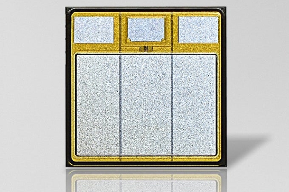
Picture: An AlN interlayer and nitrogen-radical pre-treatment increase the mobility of the GaN MOSFET
Reference
K. Ito et al. Appl. Phys Express 16 074002 (2023)