3D-Micromac shows latest tools at Semicon West
Power devices and microLEDs among applications enabled by laser micromachining solutions
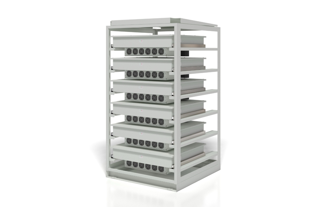
3D-Micromac AG, a specialist in micromachining and roll-to-roll laser systems, will show new developments in laser micromachining for power devices, magnetic sensors, and microLEDs at Semicon West from July 11-13, 2023 in San Francisco.
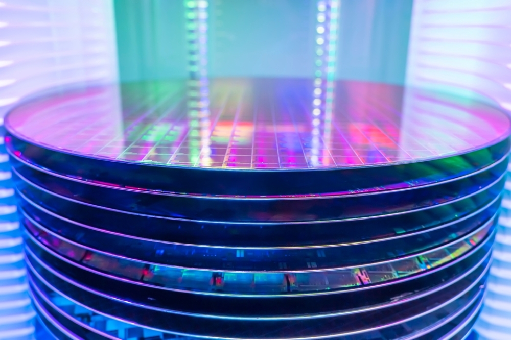
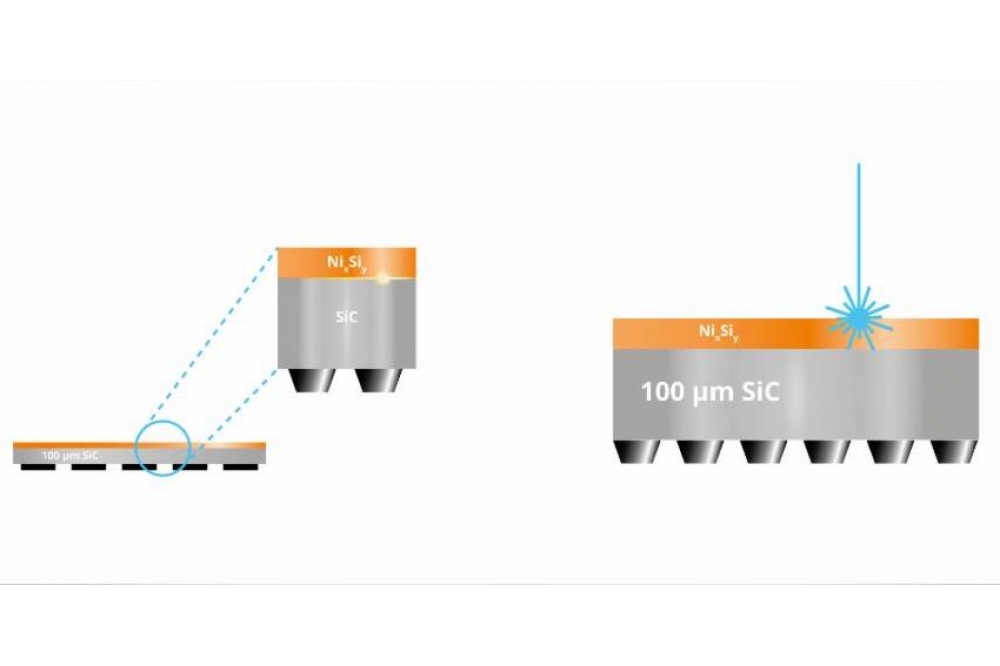
While much goes into the development of SiC power devices, the formation of ohmic contacts on the backside of these devices plays a key role in defining their electrical characteristics and mechanical strength.
The microPRO XS OCF system from 3D-Micromac is designed for ohmic contact formation (OCF) in SiC power devices due to its high precision and repeatability, and low thermal leakage, which prevent thermal damage to the wafer frontside that can negatively affect device performance. The system features a UV-wavelength diode-pumped solid-state laser source with nano-second pulses and spot scanning to process the entire metallised backside of SiC wafers while preventing the generation of large carbon clusters and heat-related damage to the frontside of the wafer.
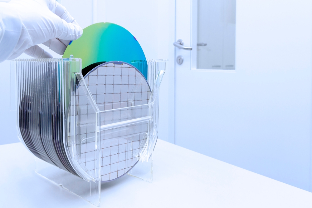
New features include a large energy density process window that ensures constant stable forward voltage; and the ability to process 200-mm SiC wafers without stitching, which avoids the creation of dead zones that can negatively impact yield and device quality
Laser-based sample preparation
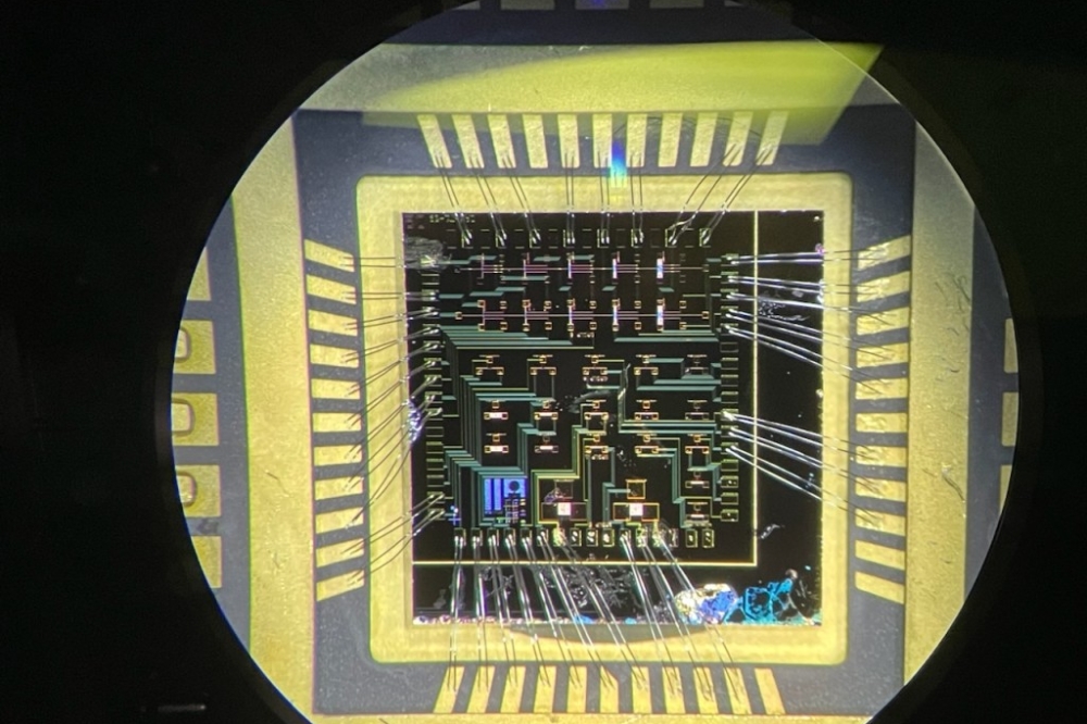
Cutting and preparing samples from semiconductor wafers, dies and packages for microstructure diagnostics and failure analysis (FA) is an essential but time-consuming and costly step. Focused ion beam (FIB) micromachining can take several hours to prepare a typical sample. In addition, FIB only allows for very small sample sizes, and wastes precious FIB time by 'digging' excavations needed for cross-sectional imaging. Reaching larger depths or widths is severely restricted by the limited ablation rate.
3D-Micromac says its microPREP PRO system now enables laser-based sample preparation for a variety of specimen preparation applications. It complements existing approaches to sample preparation by off-loading the vast majority of sample prep work from the FIB tool and relegating FIB to final polishing. As a result, the microPREP PRO significantly reduces time to final sample to less than one hour in many cases.
New semiconductor applications for the microPREP PRO include preparing chunks and wedding cake structures for micro/nano X-ray tomography, cross sections, delayering, decapping, and ablation of layers to expose wires for probing and testing. The microPREP PRO also supports microLED manufacturing by enabling lift-out of defective microLEDs for subsequent inspection and failure analysis.
3D-Micromac also recently introduced its new microPREP PRO FEMTO system, which features a femtosecond laser source and optimised optical setup to provide high-speed atom probe tomography (APT). The microPREP PRO FEMTO reduces APT sample prep time from hours to minutes with millimeter-precision while avoiding thermal damage to the sample.