Making headway with normally-off Ga2O3 transistors
Multiple sub-micron fins ensure far greater consistency in threshold voltage
A team from Novel Crystal Technology (NCT), Japan, is claiming to have made significant progress in the design and performance of b-Ga2O3 vertical transistors. The team’s normally-off devices are said to combine a ground-breaking consistency in threshold voltage with good values for on-resistance, channel mobility and current density.
This success will help to drive the progress of power devices made from b-Ga2O3. Drawing on a bandgap of 4.5 eV or more and a theoretical breakdown electric field of 6-8 MV cm-1, devices made from this oxide are promising candidates for power electronics, particularly for deployment in power conditioning, power distribution and switching applications.
The Achilles heel for Ga2O3 is its lack of p-type doping. Due to this, normally-off characteristics have been realised by turning to lateral transistors with a recessed gate and a sub-micron fin-channel. However, with this design the threshold voltage is then governed by the recess depth and the sub-micron fin width.
“Although it is technically possible to fabricate FETs with sub-micron patterns, it requires equipment dedicated to microfabrication, such as an electron-beam exposure machine,” argues Daiki Wakimoto from NCT. He explains that 100 mm and 150 mm production lines use i-line stepper exposure tools, which are less accurate and would struggle to offer sufficient control over the dimensions of the sub-micron FETs.
To overcome this issue, some researchers have investigated b-Ga2O3 high-resistive p-well-like structures, which have a threshold voltage that depends on the dopant concentration of deep acceptors. But these devices are yet to fulfil their promise: in once case, the device only operated in the sub-threshold regime; while another required a positive gate-bias of 25 V.
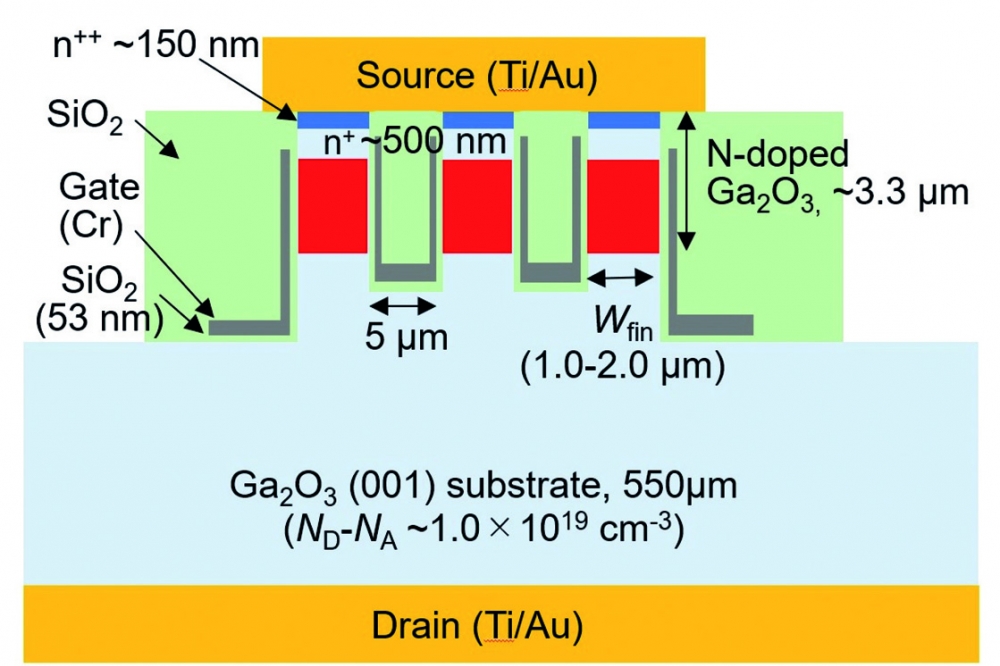
NCT’s devices, which employ several sub-micron fins with a width that has very little impact on the threshold voltage, feature a 3.3 µm-thick nitrogen-doped Ga2O3 well layer. This well is grown by HVPE on an n+ b-Ga2O3 substrate that does not have a drift layer.
Fabrication of the transistors began with two silicon-ion implantation steps, employed to connect the MOS channel to the source region, and to enable an ohmic contact to the source. A combination of mask deposition, electron-beam lithography and dry etching defined fin channels with near-vertical sidewalls, before the addition of: a 53 nm-thick SiO2 gate dielectric by atomic layer deposition; and source, gate and drain contacts by electron-beam evaporation.
The team’s portfolio of devices features fins with widths of either 1.0 µm, 1.5 µm or 2.0 µm. Each transistor has 14 fins, but only 10 are covered with the source electrode, because those on the outside often have large errors in dimension, due to what’s described as a micro-loading effect.
According to Wakimoto, the etching environment differs between the pattern’s outermost periphery and its inside. “We select conditions that stabilise the inner shape, so the error in the outer dimensions becomes larger than the inner dimensions.” This problem has been seen in other materials, and resolved by optimising etching conditions. “Therefore, we believe that gallium oxide can be improved in the same way,” added Wakimoto
Electrical measurements on the devices revealed: a threshold voltage of around 1.9 V; a current density of 760 A cm-2; an on-resistance of 2.9 mΩ cm2; and a mobility of around 100 cm2 V-1 s-1, a value that is said to be attractive for making 600 V to 3 kV MOSFETs.
Wakimoto are co-workers are now planning to increase the threshold voltage of their devices, via greater nitrogen doping, to 3 V or more, a pre-requisite for practical power devices.
Reference
D. Wakimoto et al. Appl. Phys. Express 16 036503 (2023)


