Multi-dimensional power devices
Advancing power electronics is not all about new materials.
Architectures really matter, with the likes of superjunctions, multiple
channels and multiple gates offering the opportunity to revolutionise
power devices.
BY YUHAO ZHANG FROM VIRGINIA TECH
Power Electronics is key to realising high-efficiency energy conversion in various applications, including data centres, electric vehicles, electric grids and renewable energy processing. The global market for power semiconductor devices and ICs is already worth $40 billion per annum, and it is rapidly increasing.
Many working in this sector hold the belief that to advance power devices there’s a need to introduce new materials. Transistors made from silicon should be replaced by those made from wide-bandgap semiconductors, such as SiC and GaN, and there will come a time when it’s right to move on to ultra-wide-bandgap variants, such as Ga2O3, AlN and diamond.
But my view, shared by colleagues including Florin Udrea of the University of Cambridge and Han Wang of the University of Southern California, is that innovation in device concept and architecture is equally important – and such innovation is material agnostic. This has led us to publish a roadmap late last year for device architecture innovation (for the details of that paper, see Further Reading).
History supports our position. Just track the evolution of silicon power devices before the advent of wide bandgap materials. During that era, innovation in device architecture drove the development of power electronics, from the commercialisation of thyristors in the 1950s to the power MOSFETs of the 1970s and the insulated gate bipolar transistors (IGBTs) of the 1980s. We believe that a new wave of power devices hinges on the introduction of multi-dimensional architectures.
The role of the power device is to conduct a high current in its on-state, block a high voltage in its off-state, and be capable of continuously switching between these two states at a high frequency. For conventional power devices, such as MOSFETs and IGBTs, the main current flow and the blocking electric field are aligned in same direction, rendering them as effective uni-dimensional devices.
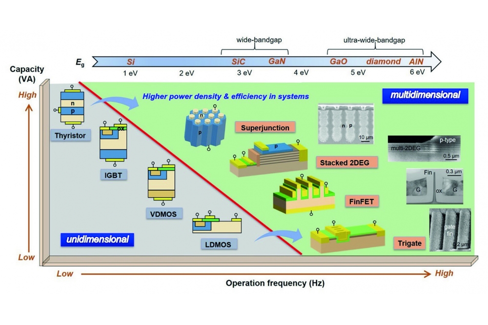
Recently, several innovative architectures have been developed that introduce electrostatic engineering in at least one additional geometrical dimension. Such architectures include super-junctions, multiple channels and multiple gates. Depicted in Figure 1, these multi-dimensional devices overcome the capacity-frequency trade-off that holds back the performance of their conventional cousins, enabling them to realise a lower power loss and a higher frequency. Armed with these attributes, designers can enhance the efficiency of their power electronics systems, while reducing the form factor.

Figure 1. Power capacity and frequency trade-off of 1D and multi-dimensional power devices.
Unipolar power devices are also hampered by another trade-off that fundamentally limits their performance: the relationship between the breakdown voltage and the specific on-resistance. As shown in Figure 2, when multi-dimensional devices are made in silicon, SiC and GaN, they can surpass their respective 1D material limits. What’s particularly encouraging is that their performance can be continuously enhanced by scaling certain structural parameters. This has spawned a new band of device limits, beyond the 1D limit line for each material. In stark contrast, most 1D unipolar power devices gain little improvement with geometrical scaling. Hence, there’s a compelling need to re-write the performance limits and the figures of merit for multi-dimensional power devices.
For superjunction devices, the electric field is modulated in a plane that’s perpendicular to the direction of current conduction. This class of power device is formed by creating alternating n-type and p-type regions. Charge balancing leads to a uniform electric field and a superior blocking voltage, regardless of the doping in each region. With this architecture, the doping level can be increased by orders of magnitude, slashing on-resistance.
Since the introduction of CoolMOS in the late 1990s by Siemens, now Infineon, the silicon superjunction has been a spectacular commercial success. And in 2016, the superjunction family welcomed a new member, in the form of SiC, with this device exceeding its 1-D performance limit.
For GaN, breakthroughs coming from the introduction of new architectures have included the development of devices with multiple two-dimensional carrier channels aligned perpendicular to the plane of current conduction. In such devices, the polarisation charges, as well as a possible additional p-type cap layer, can be self-balanced in the device off-state, fulfilling a functionality similar to that of a superjunction. Using this approach, our teams at Virginia Tech, University of Southern California, and University of Cambridge, have demonstrated multi-channel AlGaN/GaN devices blocking 10 kV, a performance that exceeds the limit of 1D lateral GaN devices.

Figure 2. Specific on-resistance and breakdown voltage trade-off of 1D
material limits and multi-dimensional power devices demonstrated in
silicon and the wide-bandgap semiconductors SiC and GaN.
For transistors operating below a kilovolt, the channel resistance can dominate the device’s on-resistance. To slash resistance, device designers can turn to multi-gate architectures and submicron fin-shaped channels. The fin is a particularly attractive option, as it shifts carrier transport away from the low-mobility surface channel, thereby increasing the overall channel mobility.
This approach is widely applicable, with trigates and FinFETs demonstrated in various power transistors, including MOSFETs and HEMTs, using multiple materials.
Late last year, working with additional collaborators, our teams broke new ground, unveiling the first vertical superjunction in GaN. This success, unveiled at the 2022 International Electron Devices Meeting, builds on the heterojunction with p-type NiO, which was sputtered conformally on the sidewalls of the GaN pillars (see Figure 3). Thanks to charge balancing between NiO and GaN, our superjunction provides a blocking voltage of 1100 V and a specific on-resistance of 0.15 mΩ cm2. This level of performance exceeds the 1D limit for GaN.

Figure 3. 3-D schematic of the vertical GaN superjunction diode and the zoom-in illustration of a NiO/GaN unit-cell (left). Cross-sectional scanning electron microscopy image of the superjunction region (right).
While we have illustrated the benefits of multi-dimensional architectures to power devices, the gain they can deliver can also be enjoyed elsewhere. For radio-frequency devices, they can deliver improvements in power, frequency, and dynamic range.
Note that we are not disputing the benefits that can be wrought be introducing new semiconductor materials. But the next time you need to build a better device, don’t just think about switching materials – also consider what might be possible with a refined architecture.
Further reading
- Y. Zhang et al. “Multidimensional device architectures for efficient power electronics,” Nat. Electronic. 5 723 (2022)
- M. Xiao et al. “First demonstration of vertical superjunction diode in GaN,” 2022 International Electron Devices Meeting (IEDM), 35.6, Dec. 2022.