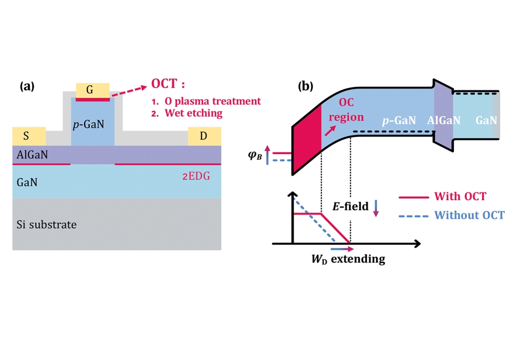
CIL expands UK packaging facility
Advanced facility can handle GaN and SiC based power modules, discrete devices and associated assemblies
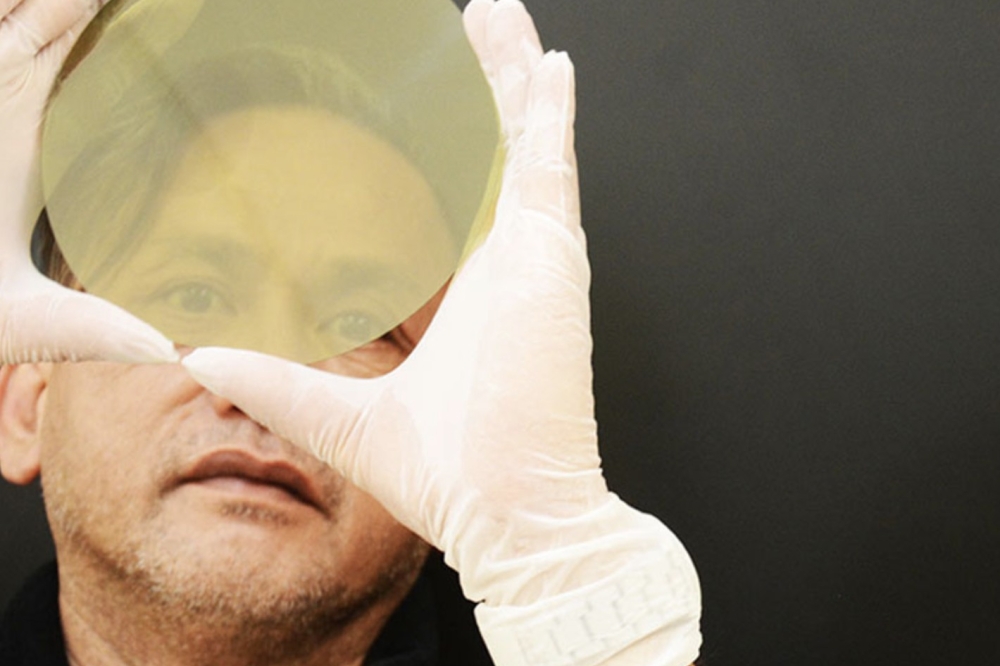
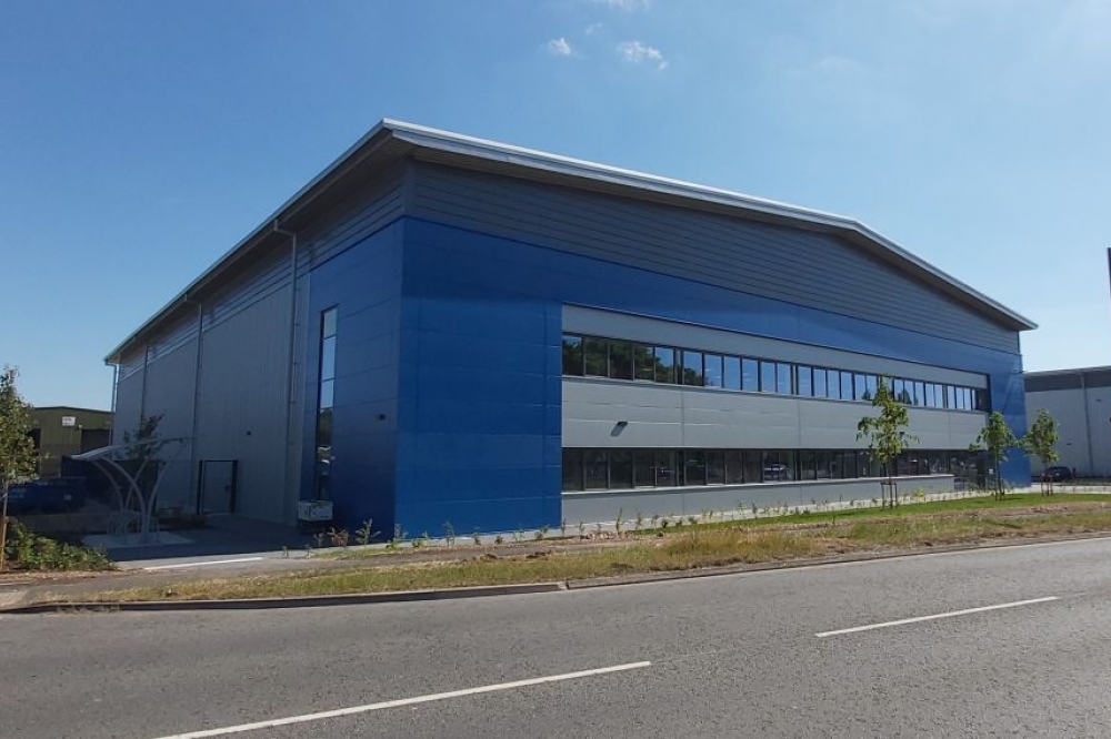
CIL (Custom Interconnect Ltd) is creating an advanced semiconductor packaging, power device and volume PCB assembly manufacturing facility in the UK. Supported by £9M in capital investment, the company is expanding its existing 34,000sq ft facility in Andover to over 80,000sq ft. Within that is a 15,000sq ft ISO7 (Class 10,000) fully qualified cleanroom which will be ready by late May 2023.
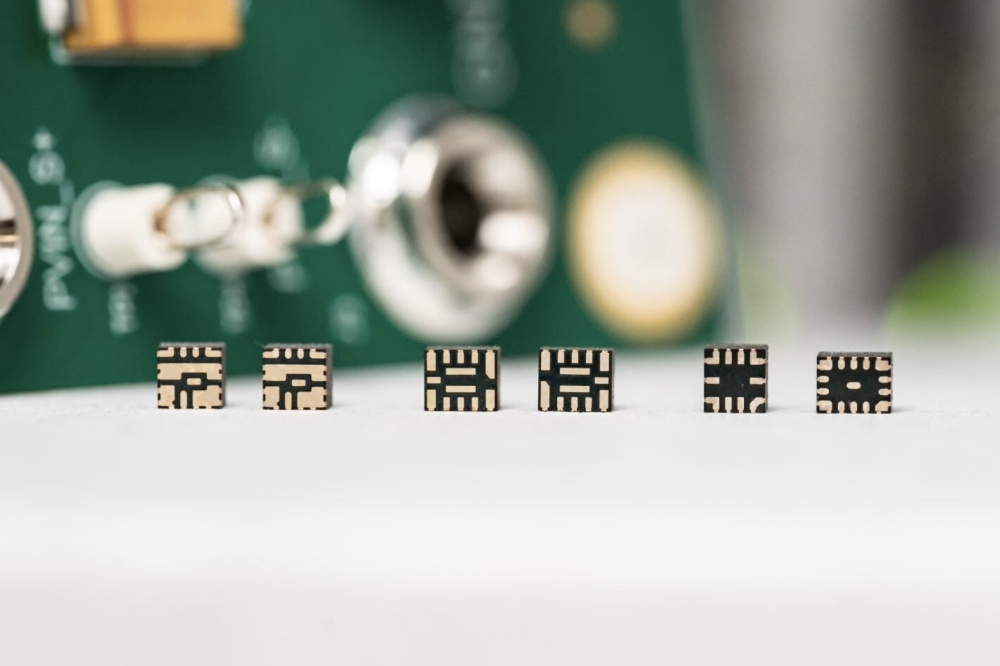
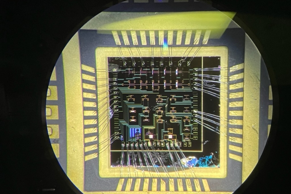
As well as the additional capacity, CIL is increasing its process capability with the addition of a DISCO DAD 3361 dicing saw, Boschman UNISTAR Automatic Film Assisted Plastic Overmold and Scheugenpflug VDS U1000 / LP804 VDU Auto epoxy fill system with more equipment and processes to come. CIL says this equipment will enable it to offer UK-based wafer dicing, full device overmold service for devices, partial device overmold and SiC and GaN based power module potting manufactured within a UK-based, UK-owned facility.
One of the catalysts to expansion has been the company's involvement in InnovateUK-supported power and compound semiconductor innovation programs. Starting with InnovateUK joint funded project 'GaNSiC' in 2019 and then followed by APC15 project '@FutureBEV' in 2020, CIL has been supporting the development of GaN and SiC based power modules, discrete devices and associated assemblies.
These two projects have led to further R&D projects that have been supported by national funding programs including the Advanced Propulsion Centre (APC), Driving the Electric Revolution centre (DER-IC), DCMS and InnovateUK. They are all focussed on more efficient power electronics in support on Net Zero. The technologies span a range of sectors including automotive, rail, aerospace and space, 5G Communications and data-centre infrastructure.
Since 2019, CIL has increased its specialist engineering department from eight to 30 engineers with further plans to double it again over the next three years. The company says this investment in engineering skills coupled with the additional unique processing equipment, will create one of the UK’s largest independent semiconductor packaging facilities, and will accommodate both world leading development labs and full volume production areas.
The UK has a thriving chip design community, but very little UK based packaging capability able to deal with development, low volume and high-volume production, CIL says the new facility is the first stage in addressing this capacity requirement.