Bidirectional GaN switches are disrupting power management

Bidirectional voltage blocking and current conduction is an important
function in overvoltage protection. How can BiGaN devices help?.
BY
THOMAS ZHAO, DIRECTOR OF R&D; DAVID ZHOU, VP OF R&D; FELIX
WANG, VP OF PRODUCT DEVELOPMENT; AND DR. JAN ŠONSKÝ, VP OF ENGINEERING
AT INNOSCIENCE.
Bidirectional voltage blocking and current conduction is an important function in overvoltage protection on USB ports, switching circuits for devices that operate from multiple power sources and high side load switches. But until now, designers have been limited to using two N type MOSFETs connected back-to-back in a common source configuration.
Such a solution requires two components and suffers from limitations related to on-resistance (RDS(on)), safe operating area (SOA) and other parameters. Innoscience’s Bidirectional gallium-nitride (BiGaN) switch is a disruptive solution that reduces power dissipation and offers a significantly smaller footprint. This article introduces our innovative BiGaN device structure, reviews the performance of BiGaN devices and elaborates on different driver configurations for BiGaN.
The integration limitations with MOSFETs are mostly a result of their vertical structure that makes it extremely challenging to put two FETs onto one die with optimised cost, RDS(on), and voltage ratings for devices rated for about 30 V and above. The lateral structures of GaN HEMTs and the lack of a parasitic body diode makes it relatively easy to create a monolithic bidirectional GaN switch.
In a smartphone, for example, replacing back-to-back MOSFETs with a BiGaN HEMT reduces on-state resistance by 50 percent, chip size by 70 percent, and temperature rise by 40 percent (Figure 1).
Figure 1. Two back-to-back Si MOSFETs are replaced by one BiGaN
Losing the losses, shrinking the footprint
The adoption of an over-voltage protection (OVP) switch in the battery management system of a smartphone is driven by the desire to reduce total losses within the minimum possible footprint. In this particular use case, the power switch is either blocking voltage or conduction current without the need for frequent switching between these two states. Hence the switching losses determined by the gate charge are not important. The total losses are determined essentially only by conduction losses, and thus device total on-resistance.
Traditionally, the OVP functionality is realised by back-to-back discrete MOSFETs. Innoscience’s solution is the BiGaN device, which is only slightly larger than a typical single GaN HEMT. It has significantly lower on resistance and is a smaller solution when compared to using two discrete devices in a bidirectional switch configuration.
For a conventional MOSFET, RDS(on) is the resistance between the drain and source when the device is fully on. The equivalent value of a BiGaN device is RDD(on) the resistance between the two drains when the device is fully on. For the 40 V INN040W048A BiGaN bidirectional switch with a drain current of 20 A, the max RDD(on) is only 4.8 mΩ, resulting in a very low conduction losses.
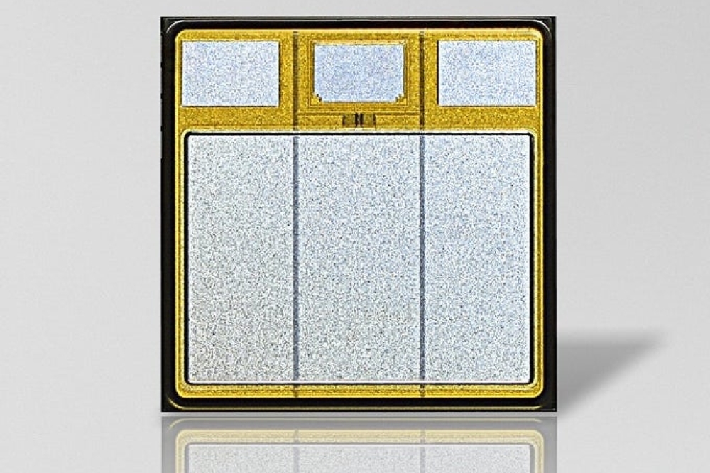
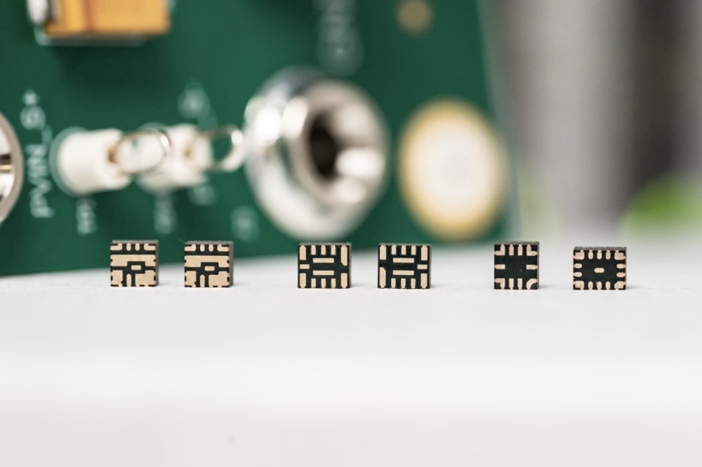
The package can be an important contributor to on-resistance. The lateral structure of BiGaN devices enables the use of a wafer level chip scale package (WLSCP) measuring only 2.1 x 2.1 x 0.54 mm INN040W048A. This package has minimal parasitic resistance, contributing to lower conduction losses and less thermal dissipation. The small package size also results in excellent on-resistance * area performance (Ron*A), an important factor in system miniaturization. And a single BiGaN device replaces two MOSFETs, further contributing to smaller solutions and a reduction in the bill of materials.
Overall, customers can make different trade-offs with Innoscience’s BiGaN devices. One option is to maintain the existing space and footprint, while significantly reducing on-resistance and consequently also limiting temperature increase during charging. Alternatively, BiGaN by Innoscience enables significant reduction in footprint for the OVP function, while keeping good on-resistance and thus efficiency.
Figure 2:BiGaN INN040W048A SOA: a) 25°C; b) 85°C.
SOA, Leakage and Robustness
SOA is an important consideration for load switching applications. It’s the combinations of voltage and current over which a device can be operated without damage or degraded performance. Factors limiting SOA include Ron, package considerations and thermal considerations. Improving the SOA of a Si MOSFET is challenging due to the negative temperature coefficient of the threshold voltage (Vth). Due to a reduced temperature dependence of VTH in GaN devices, BiGaN can maintain superior SOA performance also at high temperature (Figure 2).
Gate leakage is another important specification in bidirectional voltage blocking applications. Si MOSFETs have very good gate leakage performance. These devices have gate insulated from the channel by a gate oxideresulting in a sub-μA leakage at 25 °C. Since Si MOSFET Vth decreases at higher temperatures, the leakage current rises at elevated temperatures.
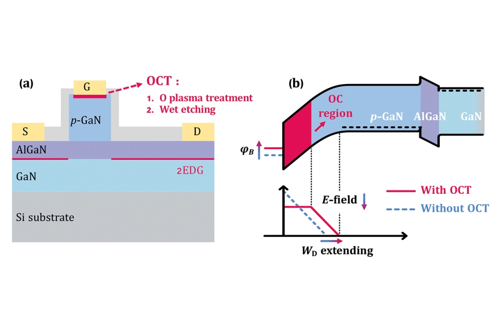
BiGaN devices have an inherently different gate structure that can be visualised as two back-to-back diodes (Figure 3). The upper diode is a Schottky structure with the gate metal as cathode and the pGaN as the anode.
Figure 3: The inherent back-to-back diodes in the gate structure require that strict process control be implemented to achieve leakage under 3 µA at 85°C for BiGaN.
The lower diode is a junction structure with a pGaN anode and an AlGaN cathode. Without proper control, the gate leakage of a BiGaN device would be higher than that of a Si MOSFET. Innoscience’s R&D team has developed differentiating process steps and process controls to ensure the gate leakage is smaller than 3 μA at 85 °C throughout the device lifetime. This was a critical requirement for its adoption in smartphone handsets.
Robust gate and drain operation are expected from all power switches. At 5.0 V (VGD) and 125 °C, the lifetime of BiGaN devices under continuous stress based on a 0.001 percent failure rate (10 ppm) exceeds 23 years. In actual applications, gate voltage spikes can be experienced from events such as short circuits.
Figure 4: BiGaN Gate robustness: a) TGDB Weibull distribution; b) Gate acceleration mode
The gate pulse capability of BiGaN devices is 10 million cycles at ≤8.5 V with a 1 µs pulse width, at 25 °C and 85 °C, and 100,000 cycles at 9.5 V and 85 °C (Figure 4). To measure drain robustness, INN040W048A devices were exposed to continue stress of 68 V, 69 V and 70 V at 125 °C. The drain time dependent dielectric breakdown (TDDB) obeys the Weibull distribution and using the most conservative approach to TDDB modelling, shows that at 32 V (VDD) and 125 °C, the lifetime based on a 0.001 percent failure rate (10 ppm) for BiGaN exceeds 10,000 years (Figure 5).
Figure 5: BiGaN Drain robustness: a) TDDB Weibull distribution; b) Drain acceleration mode.
Driving BiGaN
If the drive voltage is 5 V, existing drivers used with back-to-back Si MOSFETs can be used with BiGaN. In the case of smartphones, most charger ICs are compatible with GaN HEMTs with a 5 V gate drive. Drivers like the SC8571 from Southchip, NuVolta Tech’s NU2205, switch capacitor drivers from Texas Instruments and power management ICs (PMICs) from Qualcomm are suited for driving BiGaN.
The gate voltage needs to be at least Vth (~1.7 V) above either Drain1 or Drain2 to turn on a BiGaN device. To turn it off, and block current flow in both directions, both gate to drain voltages (VGD1 and VGD2) need to be below Vth.
Pulling the gate to ground will turn off a BiGaN device. In 5 V applications, a charge pump can be used to drive BiGaN (Figure 6). The gate voltage will be zero when EN is low and the BiGaN will be off. When EN is high, the gate voltage will be pumped to VIN + 5 V and the BiGaN will be ON and VOUT will equal VIN. In applications other than smartphones, 5 V gate driver ICs are not commonly used. Those applications use drivers with a drive voltage of about 10 V designed for getting the lowest RDS(on) from Si MOSFETs.
Figure 6: In 5 V applications, a charge pump can be used with a standard 5 V gate drive IC to turn BiGaN devices on and off.
Those drivers can’t be used to directly drive GaN HEMTs since the drive voltage exceeds the gate’s maximum rating. In these applications, a clamping circuit can be used where Zener diodes (D1 and D2) are used to clamp VGD at under 6 V. Diodes D4 and D5 have breakdown voltages over 40 V to provide drain-to-gate blocking.
Conclusion
The availability of high-performance, low-cost GaN-on-Si has enabled the development of BiGaN devices that can improve the operation of switching circuits for devices like smartphones that operate from multiple power sources, high side load switches, overvoltage protection on USB ports and similar applications.
As shown, BiGaN is reliable and easy to use. In smartphones, BiGaN can support fast charging with lower temperature rises compared with solutions using back-to-back Si MOSFETs. In addition, the small solution size when using BiGaN enables the devices to be embedded in the handset, instead of the charger, to control battery charging and discharging currents.
Taking that function out of the charger can support smaller charger designs. BiGaN is a disruptive development that is enabling new design paradigms.


