Innoscience aims high at global GaN

With new operations in the US and Europe, China's Innoscience is increasing investment and ramping 8 inch GaN-on-silicon production for worldwide markets, reports Rebecca Pool.
If you wanted yet more confirmation that GaN players anticipate significant market growth soon, China-based Innoscience recently launched design and sales operations in the US and Europe. Founded in December 2015 to develop high and low voltage HEMTs using its 8 inch GaN-on-silicon technology, the integrated device manufacturer has already shipped more than 30 million devices globally and is currently ramping production at its two China-based fabs.
As Denis Marcon, general manager of Innoscience Europe, tells Compound Semiconductor: “We have a very nice market share in China, which is getting bigger and bigger, so saw the opportunity to expand our market to Europe and the US.”
“We believe that today's customers are now ready to move full speed into GaN, which is different to how things were several years ago,” he adds.
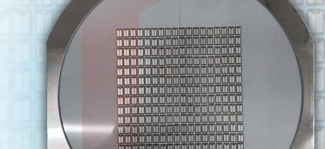
While many GaN players are currently manufacturing GaN-on-silicon devices on 6 inch wafers, Innoscience has been focused on 8 inch production from day one. Marcon highlights how company founders always believed the market would to 'explode', and wanted to make affordable chips within a large-scale manufacturing capacity and high-throughput silicon manufacturing processing that guaranteed security of supply.
With this in mind, Innoscience opened its first fab in Zhuhai in 2017 with its second, Suzhou fab, following in 2020. Combined manufacturing capacity right now is some 10,000 8 inch wafers per month - with 4000 wafers coming from Zhuhai and 6000 from Suzhou - but this figure is expected to rise to around 70,000 come 2025, as expansion at Suzhou continues.
Critically, the fabs are kitted out with the latest 8 inch manufacturing tools, including Aixtron G5+C MOCVD reactors - Marcon reckons the company can produce nearly twice as many devices on an 8 inch wafer compared to a 6 inch wafer. And the already automotive-qualified Zhuhai fab is expected to churn out devices for automotive applications come 2024.
“We really invested in production and people used to ask are you going to need that much capacity?” he says. “But now we have a lot of capacity - and huge market requests.”
Delivering HEMTS
Innoscience is currently manufacturing low voltage, 30 to 150 V, and high voltage, 650 V, enhanced-mode HEMTs. As Marcon points out, the company has worked hard to reduce specific on-resistance and shrink device size by depositing a stress-enhancement layer after gate formation, during epitaxy. He also claims both RDS(ON) and off-state leakage show excellent wafer-to-wafer reproducibility, with both wafer and device yields being high.
“Many companies focus on either low or high voltage devices - as far as I know, we are the only one that competitively offers both in several applications,” says Marcon. “And as well as performance, we offer the largest volume capabilities with strong security of supply.”
So far, power delivery and fast charging has been a key market for Innoscience, with the company also making in-roads to DC to DC conversion in data centres and LED drivers. But of course, electric vehicle markets are key, with Marcon describing LiDAR laser drivers and DC to DC conversion within electric vehicles markets as 'low hanging fruit'. “I think we will also reach 650 V on-board chargers in the near future and then of course there is the main power inverter which is where we all want to go to,” he says.
Marcon isn't overly fazed by market competition from technology-rival, silicon carbide, here. “We already have a nice history and I think the main battle, especially at 400 and 800 V, is going to be on price, and our intrinsic cost will be more competitive than silicon carbide,” he says. “But what is missing right now is 1200 V GaN - this is something that we are thinking alongside multi-level conversion as a possible alternative [solution].”
But what about GaN's age-old reliability concerns? Like many in the industry, Macon believes these are no longer a real issue. As he puts it: “There is tonnes of reliability data and we've been carrying out a lot of advanced reliability tests.”
Marcon also points to Texas Instrument's links to the JEDEC JC-70 Committee for Wide Bandgap Power Electronic Conversion Semiconductors, which recently devised test methods and circuits for continuous switching of GaN power transistors. “We really need to keep working with JEDEC on qualification, which will provide good consumer confidence,” he says.
So what now for Innoscience? Besides new US and Europe operations, recent news reports from Asia indicate the company recently won nearly CN¥ 3 billion, some £360 million, in investment funds and now intends to get GaN into as many applications as possible.
For his part, Marcon reckons it will take years for industry players, currently working with six inch wafers, to make the transition to 8 inch substrates and deliver wafer capacities that match Innoscience's present volumes. “We are not yet so well-known in the Western world but this is changing very quickly,” he says. “We are the largest IDM fully-focused on GaN technology, have more R&D engineers than many companies have employees, and want to see GaN in widespread use.”
“So we will now put ourselves in partnership mode and want to form collaborations to see how we can make this happen faster,” he adds.


