Engineering simulation can accelerate Power IC production
Standfirst: Increasing the supply of microcontroller units (MCUs),
switches and related devices is a continuing challenge as the world
seeks a reset after two years battling the COVID-19 pandemic. But as
viral variants continue emerging and manufacturers battle supply chain
headaches, Power Electronics World asked engineering simulation leader
Ansys whether multiphysics simulation can speed IC development including
the power devices needed by automotive manufacturers and many other
sectors. Ansys Director of Business Strategy Christophe Bianchi shares
his insights.
By: Mark Andrews, Technical Editor
The CHIPS for America Act. The European Chips Act. Initiatives by GlobalFoundries, Intel, Samsung, TSMC, and more – All are efforts by governments and manufacturers to grow semiconductor supplies when IC shortages of every type have dogged a global recovery following the calamitous years spent fighting COVID-19.
How are we doing? According to most measures, the semiconductor shortages faced by automotive, consumer electronics and commercial manufacturers are likely to continue through 2022 and into the first quarters of 2023. Shortages persist despite the fact that SEMI, the SIA and other global trade groups report that there are 60 semiconductor fabs under construction and that manufacturers have already increased production.
The what’s and why’s behind a persistent shortage of semiconductors have already been explored in this business magazine and many others. Essentially, getting more devices into the hands of global OEMs and contract manufacturers is going to take time. Even though the extra capacity coming online later in 2022 through 2024 will no doubt ease the crunch, can anything be done now that has not already been tried?
One place Power Electronics World sought answers was with the engineering simulation experts at Ansys, a leader in the field that is constantly expanding its portfolio of simulation services that embraces not just the ICs that fabs manufacture, but also the in-plant processes of multiple industries.

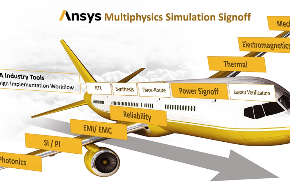
Ansys multiphysics simulation can speed the design process across device types while enabling faster review and approval cycles between team members
Engineering simulation has come a long ways since Ansys helped create the field 50 years ago. Today, engineering simulation offers the chance to test components in a virtual environment across thousands of scenarios that will materially affect device functionality, lifetime and adherence to specifications, amongst many parameters. Ansys reports that H3C Semiconductor, for example, uses the company’s multiphysics platform to engineer an advanced processor chip for cybersecurity, AI and 5G backhaul applications, effectively improving product sign-off efficiency and accelerating product development. Through simulation, it is possible to ensure that, once in service, the chips meet the reliability, performance, and longevity requirements of their respective applications, Ansys stated. According to Ansys Director of Business Strategy, Christophe Bianchi, engineering simulation is already at work to improve quality and speed production by guiding designers away from likely-to-fail scenarios while speeding design by automatically applying years’ worth of computational experience to test and verify myriad design options, materials parameters and other key metrics.
MA: Is highly accurate engineering simulation best suited for the design phase of a new product, or can it benefit other key aspects of IC manufacturing to help close the gap between supply and demand?
CB: Engineering simulation is pervasive across the entire engineering practice. Of course, the design phase is where trade-offs are made based on complex simulation, for example, thermal, mechanical, electromagnetic or Infrared. But simulation is also used to develop and optimise manufacturing processes, such as the Chemical-Mechanical Polishing (CMP) process, or tuning the performance of wafer handling in the fab. What we see becoming a critical use of simulation, combined with AI/ML technology, is the advent of digital twins of various manufacturing equipment (such as UV lithography tools). Here, the twin, running in the cloud or on the edge, provides invaluable information to pilot predictive maintenance and therefore optimise both performance and yield of these complex manufacturing processes.

Ansys simulation programmes can handle a wide variety of engineering requirements including IP validation and sign-off protocols
MA: How do today’s most advanced engineering simulation programmes differ from previous generations?
CB: Although performance and capacity remain two critical development threads in engineering simulation, for which the advent of distributed computing has provided a boost in productivity, there are two major paradigm shifts that new generations of engineering simulation impact design methodologies and product developments: Firstly, the multiphysics aspect of simulation becomes even more critical at advanced semiconductor nodes. With design margins shrinking even further, and complexity of products reaching new heights, it is now impossible to treat each phenomenon independently. The combined and interdependent effects of thermal, electromagnetic, radiation, mechanical stress, and power distribution variability must be assessed jointly in a true multiphysics way.
Another major shift is the advent of AI/ML methods assisting the designers and developers throughout their engineering tasks. With the increased complexity of today’s most advanced engineering simulations, designers must explore much more complex solution spaces, and the help provided by AI/ML facilitates those efforts by assessing parameter sensibility, and design space optimisation using automatically trained reduced-order models for faster convergence.
MA: Is it possible to estimate, if looking at a hypothetical product, how much time engineering simulation could save compared to developing said product without it or with outmoded tools?
CB: I don’t think it is a question of saving time when the alternative to simulation is prototyping. It is not just the exorbitant cost of prototyping (reaching above $1 million in advanced semiconductor nodes), but the sheer fact that the chances of silicon success without simulation is close to zero, and that is what makes engineering simulation an essential part of the design cycle. I cannot think of a situation where a design team would risk developing a product without simulation for the sake of development time.
MA: One challenge semiconductor manufacturers faced during 2020-21 that persists is addressing demand in a more agile fashion, such as rapidly changing what is being manufactured. Can engineering simulation help manufacturers rapidly retool?
CB: The IC supply crisis the semiconductor industry is currently facing is more a capacity than an agility problem. As the most affected industry by this problem, the automotive sector did not foresee the impact of “just in time” inventory practices when facing fierce competition from computing and communication for the same manufacturing capacity. These industries rebounded faster during the pandemic and secured the wafer supplies, leaving no room for peak demand from auto Tier 1s and OEMs. Running at (or slightly above) full capacity, further agility would not really solve the IC shortage crisis.
On the other hand, leveraging engineering simulation to tune and improve manufacturing yield has the potential to increase production throughout, without the delay and investment required for additional capacity. This is an area where several initiatives have been launched since the beginning of the crisis, ranging from modelling and simulation of process variability to digital twins of complete manufacturing toolchains.
MA: If better engineering simulation can indeed shorten lead times in some circumstances, are there other factors manufacturers ought to consider to address rapidly changing customer needs?
CB: In the automotive sector, the shortage of devices resulting from a combination of ultrafast demand change and a “just in time” inventory strategy have been exaggerated by the extremely large number of different components required to equip today’s cars. Calls for more standardisation and a move towards software-defined systems (using less and more standardised programmable devices) are two of the ways we are seeing improvements. But developing such multi-purpose devices brings an order of magnitude in the design complexity and requires significantly more simulation in the development and design phase.
MA: Engineering simulation has grown more sophisticated and capable. Can you please describe key breakthroughs or developmental milestones that enabled this progress?
CB: Ansys has been refining the art of engineering simulation for the past 50 years and is not planning on stopping. Our history of acquisitions demonstrates the will to combine more and more laws of nature in our multi-physics solutions: for instance, we recently added photonics and optical simulation.
The main research and development axes that have increased the capabilities and sophistication of our solutions range from continuous research in numerical methods (For example, iterative solver methods, explicit/implicit/hybrid/bayesian computational model) to AI/ML improvement of the parametrisation of our solvers, high performance computing (task-based, shared memory, message passing, fine grain (GPU) and the future use of exascale and quantum computing) as well as platforms, workflows and data management - all targeting a more pervasive use of the cloud.
MA: Can better engineering simulation enable a reduction in the number of prototypes a manufacturer needs en route to rolling out a new product?
CB: Physical prototyping, in the development of semiconductor devices, is an extremely costly and time-consuming effort. A 7nm mask set costs about $15 million (3x the cost of 16/14nm node) and prices almost double when moving down to 5nm. But this cost remains small in comparison with the total development cost of the chip. (An advanced-node large SoC development is estimated to cost around $200-$300 million). Due to the large number of parameters (and physics) that can impact a chip’s behaviour, performance and quality, simulation can provide a guarantee of convergence of the design effort, whilst solely prototyping would lead to an uncontrolled number of iterations.
MA: Could you please describe some key ways developing a new device today is assisted by Ansys software compared to development with little to no engineering simulation?
CB: Using engineering simulation enables the integration of physics constraints early in the design cycle. By taking into account the electromagnetic and Infrared effects at the planning level, designers can optimise PDNs (Power Distribution Networks) for higher performance (less DvD impact on timing), higher reliability (less fatigue and electromigration) and lower cost (optimised power grid).
What was a signoff, late-stage process in former design methods becomes a mandatory component of design planning and convergence for more complex advanced 3D ICs where multiple elements must be co-simulated in a true Chip-Package-System (CPS) view of the IR/EM/Mechanical and Thermal phenomenon impacting performance and reliability.
MA: Many of today’s advanced devices are developed by multiple engineering teams working on different aspects of the same project. How can engineering simulation aid dispersed design teams?
CB: The physics impacting a chip’s behaviour are not limited to the sub-system or component being developed by an individual contributor. These effects cross the system’s hierarchy; creating physics-true bloc and chip models (power, electrothermal, etc.,) is essential to manage parallel engineering efforts. Let’s consider, as an example, a 3D IC project that consists of 2 silicon dies in a complex package. These projects are usually split between 3 different teams (Die 1, Die 2 and Package). The computing and exchange of CPMs (Chip Power Models) of the two dies between the separate design teams is critical to avoid specific integration and EM/IR problems on each chip. This also reduces drastically the amount of data required to run the validation of each die (CPMs are compact models and replaced hundreds of Test Vectors). This issue is even more relevant when thermal analysis is to be performed as it is impossible, without using CPMs, to decouple heat emitters (dies) from the heat dissipater (package).
MA: Developing future ASIC generations often begins with what worked in a previous generation. How can engineering simulation support faster, more accurate generational evolution?
CB: The use of AI/ML to increase productivity and performance of design teams requires large amounts of data. When transitioning from Generation A to Generation B of a line of ASIC products, all the simulation and design data created in the previous generation is an extremely valuable dataset to train ML algorithms that will guide the designers in their new development. This data-driven method is becoming an essential component of the new design methodologies and must be combined with intelligent Simulation Data Management solutions to enable breakthrough productivity gains.
MA: How can engineering simulation programmes benefit the development of entirely new devices?
CB: Engineering simulation is as important in the case of a totally new product. And if historical data is lacking, our learning algorithms can automatically create the various configurations and parameter sets required to launch the simulations that will produce the data needed to build physics-informed optimisation solutions for the new design. Whether totally new or incrementally constructed, an ASIC is governed by the laws of physics and therefore must be modelled and entirely simulated, taking into account a large set of parameters (thermal, Infrared, electromagnetic, mechanical, etc.,) in order to guarantee first-silicon success.
MA: Does engineering simulation aid in IP management and sourcing?
CB: This is a very relevant question: what we are witnessing and supporting is the move towards stronger demand from IP users to IP suppliers for accurate, “true to physics” models for the IPs. These models are critical to the validation of the full system and the absence of such models can force an IP user to switch supplier. When moving from one technology node to another, even if the IP functionality remains the same, all these models have to be recreated as the physics (EM, IR, Thermal, etc.,) are highly process-node dependent.
MA: Cybersecurity is a well-established concept, but device level security design adaptations are relatively new. Can engineering simulation help designers create ICs less susceptible to corruption?
CB: In the emerging Internet-of-Things (IoT) market, data security and privacy are essential concerns for communication between a large number of ubiquitous edge devices and the internet backbone. While modern cryptography is heavily used in IoT devices to assure information security, it can be compromised by exploiting vulnerabilities in the physical implementation of underlying integrated circuits. Side-channel leakage analysis (SCLA) is a technique to extract sensitive information from sub-optimally protected hardware by probing a variety of physical phenomena, such as power consumption, electromagnetic radiation, and thermal emissions. As ICs cannot be altered in the field, it is essential to verify side-channel countermeasures in the pre-silicon design stage.

At the end of 2021, Ansys released a breakthrough technology (Ansys Redhawk SC Security) leveraging its multiphysics simulation platform that enables system-on-chip (SoC) design teams without hardware security background to predict and quantify design vulnerabilities to side-channel analysis and assess the effectiveness of their design.
But security is also a system-level concern and, across the entire electronics architecture, we are using additional technologies (named Ansys medini analyse for Cybersecurity) that carry out system-oriented cybersecurity analysis strategy to quickly identify vulnerabilities and design weaknesses, and address them to mitigate any real-world threats by implementing key security analysis methods (TOE modelling, Attack Trees, Threat Analysis and Risk Assessment (TARA), Vulnerability Analysis, etc.) in one integrated tool.

MA: Engineering simulation is rapidly evolving. Could you please consider what the future of this technology may hold for the semiconductor industry?
CB: Engineering simulation will continue to broaden its scope to all industries as we are already seeing in fields such as Healthcare (with simulation assisted surgery and, on digital twins of human organs) and agriculture (with simulation-driven crop planning and autonomous farming machines)
From an underlying technology standpoint, we will continue to leverage the innovations in high-performance computing for on-the-cloud and on-the-edge deployment of simulation, along with continuous development of data-driven physics-informed machine learning methods.
The pervasiveness of simulation is also opening new avenues for Ansys with the structuration of a developers ecosystems around the pyAnsys Framework: a community for python developers wanting to embed our true-physics solvers into their project/market specific applications for further adoption of engineering simulation.

More physics will continue to challenge our engineering minds and engineering simulation will continue to bring the necessary proof points and validation to enable more innovative products. As such, we are already deploying, with our most advanced users, simulation solutions for quantum physics, enabling what is believed to be the next revolution with quantum computing.