
Rohm releases new 20V MOSFETs
Class-leading power dissipation in a compact package ideal for small, thin devices
Rohm has recently developed a compact, high efficiency 20V Nch MOSFET, RA1C030LD, optimised for switching in small, thin devices, including smartphones and wearables such as wireless earbuds and other hearable equipment.
In recent years, the increasing sophistication and power requirements of compact devices have resulted in larger batteries that reduce the space available for mounting components. At the same time, there is a limit to the size of the battery, so to ensure more efficient use of battery power the power loss of mounted components must be minimised.
To meet this need, the development of MOSFETs in wafer-level chip-size packages (WLCSP) that contribute to greater miniaturization while maintaining the necessary characteristics is becoming mainstream in the industry. Rohm leverages its strengths as an IC manufacturer to significantly reduce wiring resistance (which has increased with conventional discrete processes). The result is a compact power MOSFET that delivers low power loss.
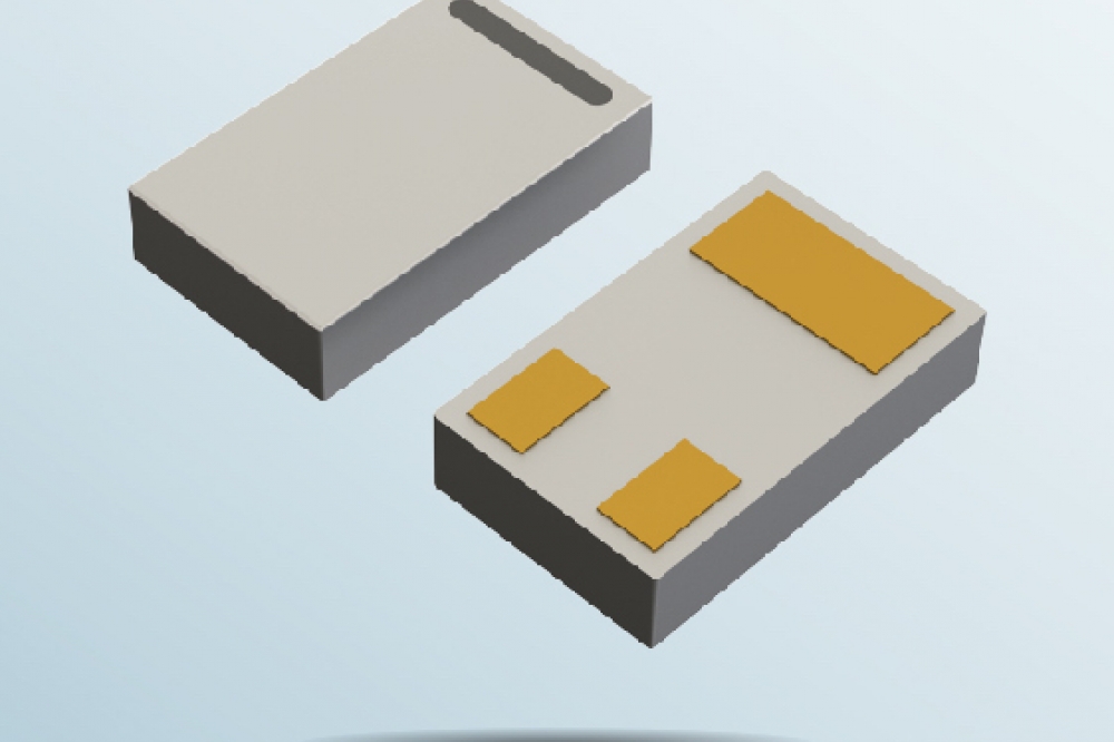
The RA1C030LD is offered in the DSN1006-3 wafer-level, chip-size package (1.0mm × 0.6mm) that takes advantage of Rohm’s proprietary IC process to achieve low power dissipation together with greater miniaturisation. In terms of the figure of merit that expresses the relationship between conduction and switching losses (ON-resistance × Qgd), an industry-leading value has been achieved that is 20 percent lower than standard package products in the same package (1.0mm × 0.6mm or smaller), contributing to a significantly smaller board area along with higher efficiency in a variety of compact devices.
At the same time, Rohm’s unique package structure provides insulated protection for the side walls (unlike standard products in the same package with no protection). This reduces the risk of shorts due to contact between components in compact devices that must resort to high density mounting due to space constraints, contributing to safer operation.


