Aehr Receives Wafer Level Burn-in System Order

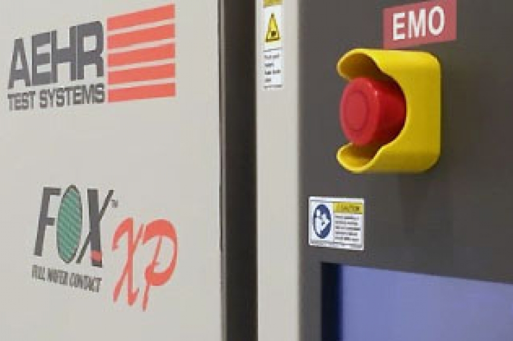
Aehr, a worldwide supplier of semiconductor production test and reliability qualification equipment, announced it has received a purchase order from a new customer for a FOX-NP multi-wafer test and burn-in system, multiple WaferPak Contactors and a FOX WaferPak Aligner to be used for qualification of Aehr’s wafer level burn-in solution for silicon carbide devices for electric vehicles and other markets. This company is a major supplier of silicon carbide devices serving several significant markets including the electric vehicle industry. This order has acceptance criteria including demonstrating certain new enhancements and functionality criteria offered by Aehr and stipulated under a corresponding evaluation and acceptance agreement. Upon successful completion of the specified criteria, final acceptance of the purchase order is met, and title transfer and invoicing will be completed.
This FOX system is configured for stress testing and burning in 150mm and 200mm silicon carbide wafers using Aehr’s proprietary WaferPak full wafer Contactors. The FOX-NP system and FOX WaferPak Aligner are scheduled to ship this week to the customer’s facility.
Gayn Erickson, President and CEO of Aehr Test Systems, commented, “We are very excited that this new customer has chosen to move forward with us after we demonstrated the capability and configurability of the FOX platform full wafer test and burn-in solution using our systems and their silicon carbide wafers at our facility in Fremont, California. This company has indicated to us that no other provider has a product that is scalable to high volume production like Aehr’s FOX-XP multi-wafer system. The FOX-NP system is a two-wafer system that is fully compatible with the volume production FOX-XP, which can be configured with up to nine or eighteen wafers depending on the customer’s specific test requirements and power configuration. This allows our customers to choose between larger and smaller configuration systems that are 100% compatible with each other at their facilities around the world. The purchase order for the FOX-NP system includes specific performance and functionality evaluation criteria that we believe Aehr will achieve on their test floor during the next three to six months which triggers final acceptance of the solution. They have provided us with forecasts for our FOX-XP systems for volume production of their silicon carbide devices at multiple facilities around the world, with initial delivery for our FOX-XP systems requested during this fiscal year ending May 31, 2023.
“Forecasts from Canaccord Genuity estimate that the silicon carbide market for devices in electric vehicles, such as traction inverters and the on-board chargers, is expected to grow from fewer than 150,000 wafers in 2021 to more than four million 6-inch equivalent wafers in 2030 to meet the demand of the automotive electric vehicle market, representing a growth rate of over 25 times the current wafer capacity just for the in-vehicle devices. Canaccord also estimates that the silicon carbide market will require an additional four million silicon carbide wafers annually by 2030 to meet demand for electrification infrastructure, industrial and photovoltaic power devices.
“The FOX family of compatible systems including the FOX-NP and FOX-XP multi-wafer test and burn in systems and Aehr’s proprietary WaferPak full wafer contactors provide a uniquely cost-effective solution for burning in multiple wafers of devices at a single time to remove early life failures of silicon carbide devices which is critical to meeting the initial quality and long-term reliability the automotive, industrial, and electrification infrastructure industry needs.”
The FOX-XP and FOX-NP systems, available with multiple WaferPakContactors (full wafer test) or multiple DiePak Carriers (singulated die/module test) configurations, are capable of functional test and burn-in/cycling of devices such as silicon carbide and gallium nitride power semiconductors, silicon photonics as well as other optical devices, 2D and 3D sensors, flash memories, magnetic sensors, microcontrollers, and other leading-edge ICs in either wafer form factor, before they are assembled into single or multi-die stacked packages, or in singulated die or module form factor.


