Henkel and CITC to Accelerate High-Thermal Die Attach Solutions

Henkel will supply pressureless sintering die attach formulations and CITC will provide materials testing and analysis
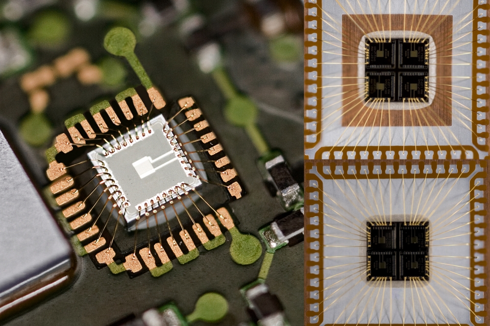
Henkel and Chip Integration Technology Center (CITC) have formalised an agreement to collaborate on the development of high-thermal die attach solutions for RF and power electronics. Under the terms of the partnership, Henkel will supply commercialised and developmental pressureless sintering die attach formulations and CITC will provide testing and analysis of the materials within next-generation package designs.
CITC’s thermal high-performance packaging program focuses on thermo-mechanical design strategies and device packaging platforms that integrate low-stress, high-reliability interconnect solutions. As die attach and molding materials are often limiting factors for the optimal operation of RF and power packages, Henkel is the ideal partner for innovation in this application area.
In addition to ongoing work in its state-of-the-art R&D centers, Henkel wants to accelerate time-to-market for its semiconductor packaging materials through strategic relationships across industry, government, and academia. CITC, which collaborates with leading power and RF device packaging companies, provides a unique opportunity to characterize and analyze Henkel’s high-thermal die attach formulations as an enabler for leading-edge device designs.
“Henkel’s pressureless sintering die attach materials are already proven in certain mobile applications,” explained Ramachandran “Ram” Trichur, the company’s Global Market Segment Head, Semiconductor Packaging Materials. “We want to extend that success to other sectors such as automotive, where large, high-power chips are the norm. Our pressureless sintering solutions are unique because they deliver the simple, low-stress processability of conventional die attach adhesives and very high thermal conductivity capabilities. The work at CITC will augment our in-house projects, allowing additional performance and reliability validation.”
The new die attach technology has the potential to enable the replacement of lead within RF and power semiconductor devices that incorporate larger die on copper leadframes, allowing the introduction of high operating temperature GaN and SiC power die technologies. Many of CITC’s partners are actively integrating these new chip structures, making the cooperative project an excellent proving ground for Henkel’s pressureless sintering platform.
“In Henkel, we have found a material innovator that will enable the development of power and RF devices with a holistic approach that leverages the latest in die attach technology,” concluded CITC General Manager, Jeroen van den Brand. “With many major power device manufacturers based in Europe, and in Nijmegen in particular, we view this partnership as vital to satisfying the current and future demands within these important market sectors.”


