Plasma-Therm Rolls Out Redesigned Heatpulse Platform

Re-engineered for demands of power devices, GaAs, GaN and SiC and ≤200mm silicon wafers
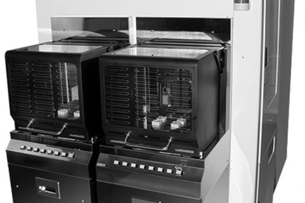
Plasma-Therm has redesigned its flagship Heatpulse Rapid Thermal Processing (RTP) platform. The move was driven by an increase in market demand for power devices, other specialty markets and ≤200mm silicon fabs.
Representing the first of several phases in Plasma-Therm’s planned technology roadmap for Heatpulse RTP, the new platform includes greater flexibility to accommodate multiple wafer sizes, upgraded robotics, and a control system backed by Cortex, Plasma-Therm’s software.
By using readily available components instead of specialised custom parts to maintain their equipment, customers can mitigate supply chain and replacement parts challenges to optimise production yields and capacity with maximise uptime during high-volume manufacturing. Additionally, the new easily implemented Heatpulse RTP wafer size conversion kits eliminate the complicated, time-consuming system hardware changes.
Like its predecessor Heatpulse 8800 and 8108 models, the new Plasma-Therm Heatpulse RTP platform can process substrates up to 200mm in diameter and can handle a diverse range of materials. This includes traditional CMOS silicon as well as compound semiconductors, such as GaAs, GaN and SiC.
The Heatpulse technology features are designed to address a multitude of semiconductor process steps, including post-implant annealing, oxide and nitride film growth, reflow, and formation of silicides, salicides, metal alloys, as well as ohmic contact formation. The Heatpulse RTP is available in either a single-oven or a new dual-oven configuration unique to the redesigned platform, and features a multi-zoned, independently controlled temperature capability.


