
Novel field plate boosts the blocking voltage
Reducing the electric field strength in the SiO2 layer increases the breakdown voltage of β-Ga2O3 Schottky barrier diodes
A team from Japanese has increased the blocking voltage of its β-Ga2O3 Schottky barrier diodes by introducing a staircase field plate on a deep trench that is filled with SiO2.
This new archirecture, realised by researchers from the National Institute of Communications Technology (NICT) and Tokyo University of Agriculture and Technology, has increased the diode’s blocking from 1.43 kV to 1.66 kV.
The success by the team is another step towards fulfilling the promise of β-Ga2O3 power devices. Diodes and transistors produced from this oxide have the potential to outperform those made from SiC and GaN, while manufacture could be inexpensive and relatively simple, thanks to the availability of native substrates grown from the bulk.
One downside of the Japanese team’s latest diode is that its high blocking voltage has come at the expense of an increase in the on-resistance, which climbed from 4.7 mΩ cm2 to 7.6 mΩ cm2 with the introduction of a new architecture.
According to team spokesman Masataka Higashiwaki from NICT, if the blocking voltage could exceed 2 kV while the on-resistance were kept below 5 mΩ cm2, this would be an important accomplishment for the power device community.
Success in this regard may be just around the corner, given that the relatively high-resistance associated with the high-blocking-voltage device did not come from a fundamental issue. Instead, it originated from a weakness in processing: incomplete removal of the surface-depleted-region formed during annealing. “We consider that it is relatively easy to decrease the on-resistance by just optimizing the process conditions a little more,” remarked Higashiwaki.
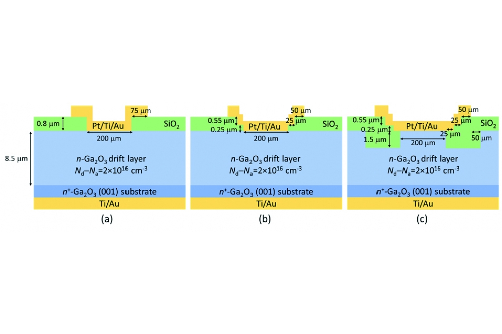
The team identified the superior architecture for their β-Ga2O3Schottky barrier diode by fabricating and investigating three different designs: the control with a conventional field plate, and variants with a staircase field plate and a trench staircase field plate.
Modelling all three designs with Silvaco Atlas software showed that for the architectures with the conventional field plate and the staircase field plate, blocking 2 kV would cause the peak electric field in the SiO2 layer to hit 12.9 MV cm-1 and 12.8 MV cm-1, respectively. As the theoretical breakdown electric field for SiO2 is just 10 MV cm-1, both designs are likely to fail below 2 kV. A better performance can be expected for the trench staircase field plate architecture, as this has a peak electric field in the SiO2 layer of 10.0 MV cm-1 when blocking 2 kV.
Devices with all three designs were formed by growing a 13 µm-thick n-type Ga2O3 layer by HVPE on an n+ Ga2O3 (001) substrate. Diode fabrication required several steps, including etching, plasma-enhanced CVD of SiO2, and the addition of metal contacts by evaporation and lift-off.
Higashiwaki said that even the process used for forming the trench staircase field plate architecture is not that complicated. “It is acceptable even for mass production.”
Measurements of breakdown voltage reflected insights provide by simulation, with the diode with the conventional field plate failing at 980 V, the variant with the staircase field plate breaking down at 1530 kV, and that with a trench staircase field plate able to withstand up to 1660 V.
Benchmarking the most impressive device showed that it produced state-of-the-art values for the combination of breakdown voltage and on-resistance.
While even higher values for breakdown voltage have been reported by a team at Cornell using simple trench Schottky barrier diodes, this came at the expense of a higher on-resistance.
Remarking on the pros and cons of different designs, Higashiwaki said: “The simple trench Schottky barrier diodes developed at Cornell are suitable for enhancing the breakdown voltage; however, the active area becomes small, leading to an increase in on-resistance.” Note that with the trench staircase field plate design, there is no sacrifice in the active area.
The team always intended to apply the etching process developed for their Schottky barrier diodes to vertical FETs. They are now pursuing that goal.
Reference
S. Kumar et al. Appl. Phys. Express 15 054001 (2022)
Pictured above: The β-Ga2O3Schottky barrier diode with the trench staircase field plate (c) can withstand a higher blocking voltage than the variant with a staircase field plate (b). The lowest blocking voltage comes from the diode with the conventional field plate (a).


