
High-voltage Ga2O3 transistors surpass silicon limit
4.4 kV Ga2O3 MESFETs with a sandwiched dielectric field plate deliver a figure of merit exceeding 100 MW cm-2
A US collaboration claims to have set a new benchmark for Ga2O3 power transistors. A partnership between the University of Utah, the University of Buffalo, Agnitron Technology and UCSB says that its MESFETs are the first Ga2O3 transistors with a breakdown voltage in excess of 4 kV that surpass the theoretical unipolar figure-of-merit for silicon.
Comparing their device’s performance with that of SiC is not easy, due to differences in geometry – most SiC devices are vertical, while the Ga2O3 MESFET has a lateral architecture.
The initial results are encouraging. “If we compare with SiC lateral devices, our devices offer half the device footprint for a higher breakdown voltage,” says Sriram Krishnamoorthy from UCSB.
However, he warns that it is still too early for meaningful comparisons between gallium oxide, which is barely a decade-old technology, and the more mature, commercial, SiC technology.
The team’s success has come from avoiding etching damage in the active region, which is the area between the source and drain contacts.
Most developers of Ga2O3 transistors employ a field plate to reduce the peak electric field and boost the breakdown voltage. However, when they fabricate this design, it leads to etching-related damage that degrades conductivity in the active region, leading to a hike in on-resistance and a reduced on-current.
“We have employed a process flow that avoids any dry etching of the active region, except for the region where the contact layers are regrown,” remarks Arkka Bhattacharyyafrom the University of Utah, adding that this ensures a low on-resistance and a high on-current.
Field plates were formed without damage to the active region through a combination of metal evaporation and plasma-enhanced CVD of SiN.
Measurements on a MESFET with a 34.5 µm gate-to-drain length, which has a gate length of 2.4 µm and a gate-to-source distance of 1.0 µm, revealed a maximum on-current of 56 mA mm-1, an on-resistance of 385 Ω, a maximum transconductance of 6.2 mS mm-1, and a sub-threshold swing of 186 mV dec-1.
Breakdown measurements, made by submerging the wafer in a dielectric liquid, provided values of 4415 V for the device with a 34.5 µm gate length, and 4567 V for the variant with a 44.5 µm gate length. This pair of devices had specific on-resistances of 148 mΩ cm2 and 219 mΩ cm2, and corresponding power figures-of-merit (defined as the square of the breakdown voltage, divide by the specific on-resistance) of 132 MW cm-2 and 96 MW cm-2. These values surpass the theoretical limit for silicon, a feat previously restricted to devices with breakdown voltages below 4 kV, according to benchmarking by the team.
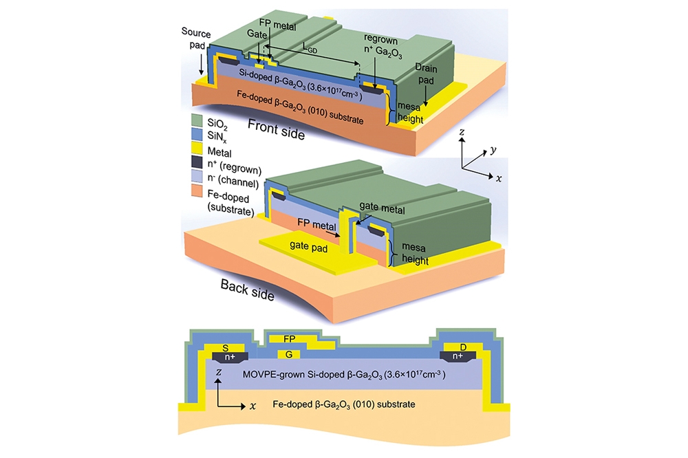
Pictured above (top to bottom): The MESFETs incorporate a field plate (a). For devices with gate-to-drain lengths of 34.5 µm and 44.5 µm, field plate extensions are 3.2 µm and 3.5 µm, respectively. The gate field plate metal is electrically connected to the gate pad outside the mesa (b). A 2D cross-section of the device along the x-z plane (c).
The collaboration are now planning to investigate alternative passivation materials and strategies that improve channel mobility while suppressing reverse leakage.
“One can also employ a gate oxide and operate in accumulation mode, and this can further reduce the on-resistance, via a higher current density,” says Krishnamoorthy.
Reference
A. Bhattacharyya et al. Appl. Phys. Express 15 061001 (2022)


