
Are GaN RF devices reliable enough for space missions?
Can concerns over the likes of intrinsic and extrinsic reliability,
mechanical integrity and radiation hardness scupper the chances of GaN
HEMTs from being deployed on lengthy satellite missions?
BY John Scarpulla FROM The Aerospace Corporation
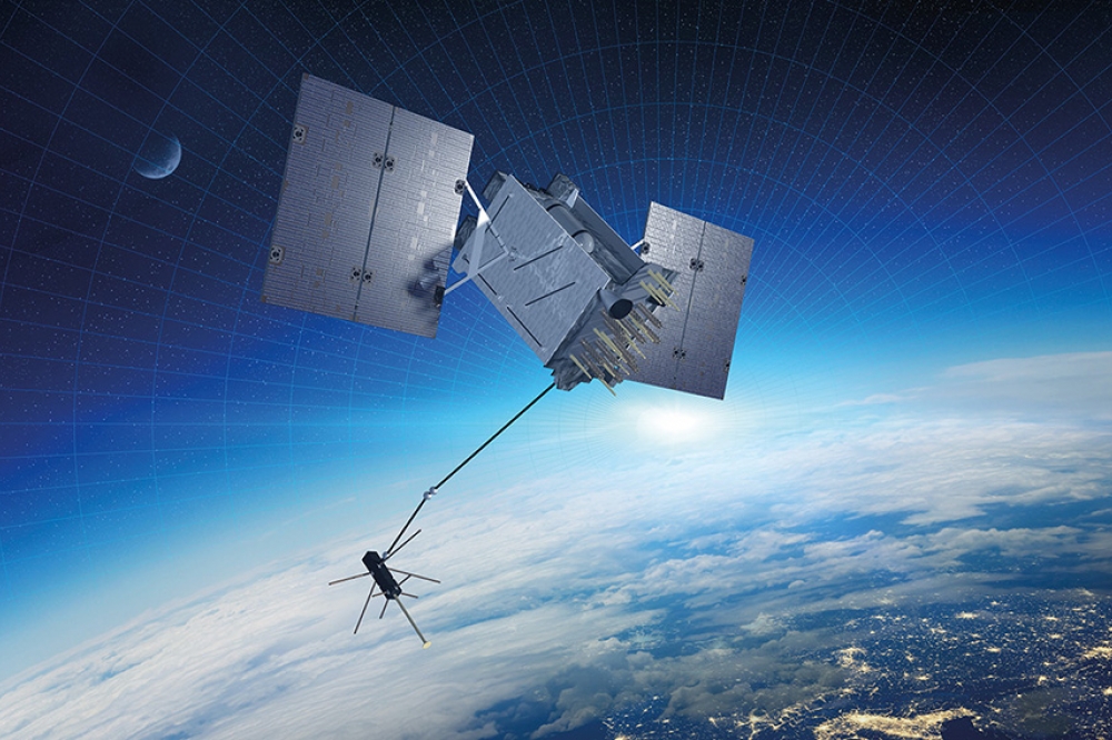
Main Image: Artist rendering of a GPS III satellite deployed in a medium-earth orbit (MEO). Credit: The Aerospace Corporation.
It is now beyond question that GaN-based microwave devices, that is transistors and MMICs, offer a high enough level of maturity to be deployed in many terrestrial and airborne applications. However, they are have yet to be incorporated in space satellite missions lasting up to 15 years, where ultra-reliability is paramount.
A lack of deployment in these space missions is certainly not due to any issue associated with performance. When GaN HEMT-based devices are used to construct power amplifiers, they outpace the GaAs HEMTs of the previous era by a substantial margin, delivering far higher power densities while operating at higher temperatures and voltages. Hunt for the details and you’ll find that when judged by those crucial metrics, GaN HEMTs offer about a ten-fold hike in the current-per-unit-gate-width when compared with their GaAs equivalents, while running at a channel temperature of 200°C or more and handling higher RF peak voltages – currently ranging from 50-100 V, and rising. And given that the overriding goal for satellite designers is to minimise size, weight and power, it would appear that GaN-based HEMT devices would be a shoe-in. But it is still a struggle to infuse high-reliability satellites with this technology. Why?
Based on my experience in working in the aerospace industry – my current role is Technical Fellow of The Aerospace Corporation – I have concluded that part of the reason why GaN is not as successful as it should be is that the existing crop of military and industry standards are not up to snuff. When specifying and acquiring high reliability semiconductor devices, the entire set of standards that’s employed are inappropriate, having been developed over the last 50 years.
Back in the 1960s and 1970s, when these standards were conceived, silicon bipolar transistors were the RF power device of choice. Since then several alternatives have emerged, including LDMOS, Si-Ge CMOS, GaAs HBTs, GaAs MESFETs, GaAs pHEMTs and now GaN-based HEMTs. Over that timeframe GaAs and InP HEMTs have rose to prominence in low-noise amplifiers, and for a GaN HEMT and MMIC, the power amplifier is now seen by many as the ‘killer app’. Failing to keep pace are the semiconductor device testing and quality standards – and compounding the issue are the additional stringent requirements for high-reliability space missions, such as radiation exposure, temperature cycling, RF multipaction, hermeticity and long mission durations. The upshot is that the problem has become even more intractable.
To try to bridge this gap I have worked with colleagues at The Aerospace Corporation – plus a working group consisting of industry, government, space contractors, GaN fab houses and academia – to develop a guideline to aid in the specification, testing and qualification of GaN HEMT-based devices for high reliability space applications. This effort has culminated in the publishing of a 205-page document, available to the general public upon request, that covers six main areas: intrinsic reliability, focusing on the identification of wearout failure modes intrinsic to all devices; extrinsic reliability, involving the characterization of defect densities affecting reliability; electrical robustness, considering the safe operating area for the gate and drain; environmental factors unique to space, such as multipaction and hydrogen poisoning; mechanical integrity issues, such as bondwires operating at higher than traditional temperatures; and radiation effects, involving considerations of radiation test plans for various environments.
In the remainder of this feature I present some highlights and key topics from this guideline. But just before we get there, I wish to emphasize that in general, to assess the reliability of an electron device one has to generate failures in a controlled and accelerated stress environment, because this allows a distribution of failure times to be extrapolated to more benign usage conditions. While tests that produce no failures may at first glance appear to be a positive result, they are not especially useful in determining the physics of failure. It is this philosophy that has been adopted for considering the qualification of GaN HEMTs.

Fig 1. GaN HEMTs suffer from many different failure mechanisms. The more common ones are depicted here, with current arrows showing electron currents. Positive and negative charges may accumulate as well as surface traps. Abbreviations used are: SCFP for source-connected field plate, TDDB for time dependent dielectric breakdown, 2DEG for two-dimensional electron gas, and TBR for thermal barrier resistance.
Intrinsic and extrinsic reliabilities
To improve the reliability of the GaN HEMT, many designers add a field plate to reduce the peak electric field on the device’s drain side (see Figure 1 for such a design, plus a list of many failure mechanisms). While this type of device could fail for many different reasons, it will not exhibit all of these traits, because they are activated under different usage or stressing conditions. The trick is to identify the mechanism, or mechanisms, that will govern wearout reliability in any given space mission scenario.
Engineers tend to operate RF power amplifiers into compression, as this increases the power-added efficiency. Depending on whether the amplifier operates in Class A, AB, F-1 or another mode, there can be a dramatic variation in the ‘load figure’ (a generalization of the load line) on the IV-plane (see Figure 2, which depicts typical load figures and illustrates how the IV plane is traversed differently depending upon the amplifier design). It is now understood that failure modes are different at different locations on the IV plane. Our working tenet is that DC stressing at the different quiescent points (or ‘Q-points’) shown in Figure 2 uncovers different failure modes. One example of this is the off-state, zero current, high-voltage condition (Q-point #4 in the figure) – this leads to voltage or piezoelectric strain-driven failure modes that cause surface pitting and trap generation.
In comparison, an on-state, low-voltage, high-current condition (Q-point #2) engenders current-driven failure modes, such as contact voiding or electromigration. The other two Q-points are ‘semi-on’ (Q-point #3), and the traditional central point in the IV-plane (Q-point #1). That’s traditional in the sense that 20 years’ worth of reliability testing of GaAs low-noise amplifiers has been performed there – an effective strategy for small-signal GaAs low-noise amplifiers, where gate sinking has been the dominant failure mode.
With GaN, there’s a need to broaden thinking to include many more failure modes. My view, and that of my collaborators, is that it is best to use DC testing: we advocate beginning with step-stress testing, before turning to constant-stress testing, to uncover multiple GaN failure modes. We also recommend ‘test-like-you-fly’ RF-driven life-testing, as this helps to correlate DC results with actual RF usage conditions. Note that more details on qualification test plan recommendations are provided in our guidelines.

Fig 2. DC (lines) and pulsed IV (points) characteristics of an RF power GaN HEMT, and representative loadlines, with four proposed operating Q-points for DC reliability testing. The shaded region above critical voltage Vcrit may exhibit quite different electric field-driven failure modes than the region below it, where thermally driven mechanisms may prevail.

Fig 3. An example of drain IV plane and common-source characteristics of a GaN HEMT showing the safe operating area (SOA), which must be extremely conservatively defined for high-reliability space missions. The dots show the burnout points that must lie well outside the drain SOA. The critical voltage Vcrit defines the onset of time-dependent degradation. A possible amplifier Q-point is shown, and Point C shows a recommended stressing condition in the guideline for power cycling tests.
Extrinsic failure modes represent the other side of the coin, producing early failures in a subset of the device population. According to JEDEC standard JESD65B, an extrinsic mode is ‘a failure mechanism that is directly attributable to a defect created during manufacturing’. Examples of such defects include particles, voids, and lithography errors.
The good news is that many of these failure modes may be screened out with appropriate tests, such as those recommended in our guideline. For example, if a particle or an irregularity is in the gate-drain recess region, this can lead to a premature breakdown of the device at the peak RF voltage – and screening HEMTs with a combination of an elevated drain voltage and temperature offers an effective
solution.
It is also possible to screen the metal-insulator-metal capacitors (MIMCAPs) that are present in MMICs. Some have argued that the reliability of a large GaN MMIC could be dominated by MIMCAP extrinsic failures rather than the HEMTs themselves. Detailed in our guideline are methods involving the use of test structures, such as large-area MIMCAPs and wide HEMTs, to estimate defect densities and their associated reliability.
Safe operating areas
When deployed on space missions that demand that all devices have a high level of reliability, it is crucial to conservatively define the safe operating area of a power GaN HEMT. In Figure 3, which shows the typical drain safe-operating-area for a GaN HEMT, plotted points depict where the device burns out abruptly as the voltage or current is raised.
One of the common characteristics of the RF GaN HEMT is that it lacks a well-defined sustaining avalanche breakdown voltage. Instead, the voltage breakdown tends to be abrupt and catastrophic. Due to this, our guidelines recommend selecting a value for the maximum safe peak drain voltage of no more than one-half to one-third of the burn-out voltage. Similarly, for conservatism, we advise adopting a similar constraint for the maximum drain current.
Those that employ GaN HEMTs should be aware that a critical voltage may exist for this class of transistor, where time-to-failure begins to be controlled by a voltage or an electric field rather than by the temperature alone. If this is the case, as well as elevated temperatures providing an accelerator for failure times, drain voltages have this effect. In our guideline we propose various models for estimating reliability, based on both temperature and voltage.
Hermetic or not?
Traditionally, it has been the case that electronic modules, and certainly RF amplifiers, are packaged hermetically for space. There are many reasons for this, including avoiding moisture effects, preventing possible solvent incursions during payload integration, and ruling out contamination from the dirty launch environment.
For GaN HEMT based RF amplifiers, the benefits of hermeticity may be dwindling. Take the maximum permissible water vapour content within a hermetic module, a figure of 5,000 parts-per-million-volume (ppmV). This requirement is designed to prevent condensation of liquid water on die surfaces. The dewpoint of internal gas that contains 5000 ppmV of moisture at 1 atmosphere lies below the freezing temperature of water, reducing the possibility that a film of liquid water might form on a die surface.
It was hoped that would prevent corrosion mechanisms in the poorly passivated silicon die of yesteryear. Now, in the era of GaN RF amplifiers, that level of moisture may not be acceptable. The issue is that GaN, as well as its family of related alloys, can react with water vapour to produce ammonia. If this reaction proceeds to produce gallium oxide and ammonia, 5,000 ppmV of water can be converted into as much as 3,333 ppmV of ammonia gas.
Note that this is not just a theoretical concern. In sealed microwave modules containing GaN devices high levels of ammonia have been found. This gives rise to two open questions: Is it acceptable to trap moisture that converts to ammonia inside a hermetic microwave module? And are the present requirements unsuitable for GaN HEMTs?
There is the possibility that vented modules containing GaN die are more reliable for space missions. One argument in favour of this relates to multipaction and ionization breakdown. All hermetic modules leak to some extent, and when launched into space, internal gas will slowly leak away. This will produce a drop in internal gas pressure and an alarming reduction in the Paschen gap – this is the distance between two electrodes needed to induce electrical breakdown by gas ionization at a particular voltage. When this gap gets too low, breakdown may take place, either between two adjacent bondpads or two adjacent bondwires acting as electrodes. This catastrophic ionization breakdown tends to occur late in a mission when the gas is leaked away.
To avoid this difficulty, the gas can be removed altogether, leading to the flying of a fully vented module resulting in vacuum after launch. But care is needed, as there is the threat of the multipactor effect: it occurs in vacuum when electrons emitted from metal surfaces, either thermionically or via field emission, resonate with an RF field, leading to electron avalanche and catastrophic damage. The cure is the combination of a well-chosen geometry and the suppression of surface electron emission by coatings or foams. In our view, a reasonable approach for space missions might be to use a high-reliability vented microwave module that is free of ionization breakdown and ammonia build-up, and features multipaction mitigation.
Radiation effects
One commonly held view is that GaN HEMTs and MMICs are ‘intrinsically’ rad-hard. This position stems from the fact that current conduction is via minority-carrier only in the two-dimensional electron gas (2DEG). Minority carrier (hole) lifetime that may be degraded by radiation is of little consequence in a GaN HEMT.What’s more, there are no gate oxides or field oxides to trap charges, like there are in silicon devices. GaN or AlGaN surfaces are Fermi-level pinned by large surface trap densities, so the radiation-induced charges in adjacent passivation layers have little effect. The upshot is that in GaN, the usual total ionizing dose of radiation and displacement damage effects are usually fairly inconsequential.
However, for those that are considering using GaN HEMTs in space, concerns should be directed at single-event effects caused by trapped electrons and protons in the Van Allen belts, and cosmic rays emanating from deep space, which are nuclei stripped of all electrons. There is plenty to consider, now that that GaN RF power devices are being propelled to higher and higher peak RF voltages.
When an ion strike occurs, it leaves behind an ionized track of semiconductor atoms. The electrons thus freed by this are capable of causing burnout, coming from the generation of current under a sufficient electric field. This ‘single-event burnout’ is now a significant concern in GaN RF power devices.
To determine how susceptible these devices may be to this form of burnout, they can be assessed using cyclotron particle accelerators. Qualification testing in this manner has shown that for a GaN device to be usable in some space radiation environments, it must be severely derated. The burnout-free operating voltage must fall to 30 percent or less of the rated voltage in some cases. To help shine more light on this major source of concern at the system level, in our guidelines we have detailed prototype radiation test plans that are suitable for space-qualifying GaN HEMTs and MMICs.
While there are concerns related to intrinsic and extrinsic reliability, electrical robustness, environmental factors, mechanical integrity and radiation, we believe that RF GaN HEMT-based devices can be qualified for high reliability in space. Addressing a combination of absence and inappropriateness surrounding space qualification tests and methodologies for GaN RF HEMTs and MMICs in existing electronic device specifications is our published guideline.
We believe that this document will help to speed the adoption of RF GaN HEMTs and MMICs for space. While new GaN standards and requirements are now being discussed by standards agencies, such as JEDEC, IEEE, ASTM, AEC and NASA, their focus is not necessarily on ensuring high-reliability in space.
Trying to fill this void, manufacturers have stepped in, developing their own test methods and qualification. But this leads to a lack of standardization, slowing the adoption of RF GaN for high-reliability space systems. It is our hope that our guidelines will help to alleviate this situation and spark the development of an industry standard for qualification of GaN RF HEMTs and MMICs for high-reliability space missions.
Recommendations for qualification methods to determine the reliability of passive devices, such as thin-film resistors, MIMCAPs and backside vias.
A checklist for qualification testing, as well as ‘50 questions’ to consider when choosing a GaN HEMT vendor or process, as a guide to the space community.


