PCB Depaneling: Laser Technology Improves Quality and Efficiency for Automotive Applications

LPKF laser systems cut printed circuit boards with technical cleanliness and maximum precision
The laser offers tremendous potential as a noncontact tool for manifold applications in the automotive industry. For PCB depaneling for the industry, use of laser technology promises high quality, flexibility, and cost efficiency.
Nearly everywhere you look in a vehicle, you’ll find printed circuit boards: in the onboard electronics and sensors, in the lighting system, in previously purely mechanical systems such as seat or mirror adjusters, and in many other in-vehicle applications. Especially for safety-relevant applications, a printed circuit board has to meet high quality standards. Here, it is essential that the PCB works reliably at all times during operation. In order to ensure this, every single detail of PCB production must be just right. With extensive expertise in laser technology and experience in the automotive industry, LPKF has these requirements in mind when it comes to depaneling and allows this know-how to flow continuously into product development.
During depaneling, the last step in the process of manufacturing PCBs, the boards in a panel are singulated. Unlike mechanical depaneling processes such as milling or punching, the laser process leaves no dust on the populated boards, so later functionality in use is not jeopardized. The depaneling process is gentle; the mechanical and thermal stresses introduced into the components by the laser are negligible.
Standards pertaining to technical cleanliness – such as VDA 19 / ISO 16232 – can be met with laser technology. LPKF's CleanCut technology enables substrate processing free of carbonization and discoloration. The result is high-quality printed circuit boards with maximal technical cleanliness. The process thus provides a preventive measure against potential component failure during use. Especially for sensitive components such as sensors, the yield for users is thus particularly high.
Laser-processable materials range from standard applications such as FR4, flex, or ceramics all the way to insulated metal substrates (IMSs) and systems-in-packages (SiPs). With adjustment of the parameters, the same tool can be used for flexibly processing a wide range of materials and material compositions.
This diversity of compatible materials for technically clean and precise laser depaneling allows the PCBs to be used in a wide variety of application environments: from the heat and cold found in the engine compartment or sensors in the chassis to pressurized environments found in the tires.
There are virtually no restrictions on the design of the printed circuit board: contours do not need to be straight and there are no minimum radii, tabs, or similar limitations. The pinpoint control of the laser beam results in unsurpassed cut precision and extremely narrow cutting channels. With a full-perimeter cut, the individual printed circuit boards can be positioned on the panel without large breakout clearance channels for optimal space utilization. Thus, materials savings of more than 30% in comparison with mechanical depaneling processes can be realized. This paves the way for achieving cost efficiency in the production of application-specific printed circuit boards – and additionally has a positive effect on the ecological footprint.
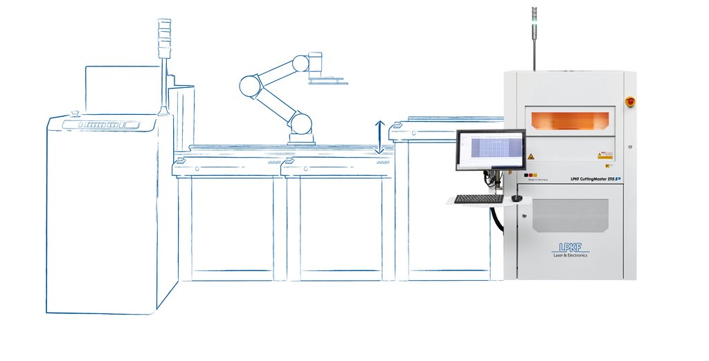
Laser systems such as the LPKF CuttingMaster can easily be integrated into existing manufacturing execution systems (MESs). With the sophisticated software, a high process stability is achieved. The extensive automation of the laser systems simplifies handling. Thanks to the higher power of the integrated laser sources, today’s laser machines can fully compete with mechanical systems in terms of cutting speed.
The operating expenses of a laser system are low. There are no noteworthy wear parts such as milling heads. Thus, ongoing parts costs and production downtime for replacing parts are a thing of the past.
Besides being used for substrate cutting, the laser can be used for marking, drilling, or ablation of individual material layers.


