
GeneSiC announces 6.5kV SiC MOSFETs
Chips offer performance, efficiency and reliability in applications such as traction, pulsed power and smart grid infrastructure
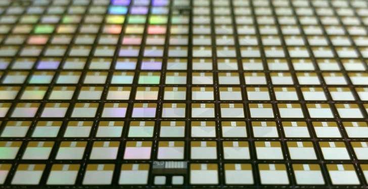
GeneSiC Semiconductor, a US maker of SiC power semiconductors, has announced the immediate availability of 6.5kV SiC MOSFET bare chips – G2R300MT65-CAL and G2R325MS65-CAL. Full SiC modules based this technology are also soon to be released.
Applications include traction, pulsed power, smart grid infrastructure and other medium-voltage power converters.
GeneSiC’s innovation features a SiC double-implanted MOSFET device structure with a junction barrier schottky (JBS) rectifier integrated into the SiC DMOSFET unit cell. Other significant advantages include more efficient bi-directional performance, temperature independent switching, low switching and conduction losses, reduced cooling requirements, superior long-term reliability, ease of paralleling devices and cost benefits.
"GeneSiC’s 6.5kV SiC MOSFETs are designed and fabricated on 6-inch wafers to realize low on-state resistance, highest quality, and superior price-performance index. This next-generation MOSFET technology featuring an on-chip integrated JBS diode promises exemplar performance, superior ruggedness and long-term reliability for medium-voltage power conversion applications" said Siddarth Sundaresan, VP of Technology at GeneSiC Semiconductor.


