Looking inside SiC transistors to save energy

FAU team finds defects in power transistors more accurately, quickly and simply
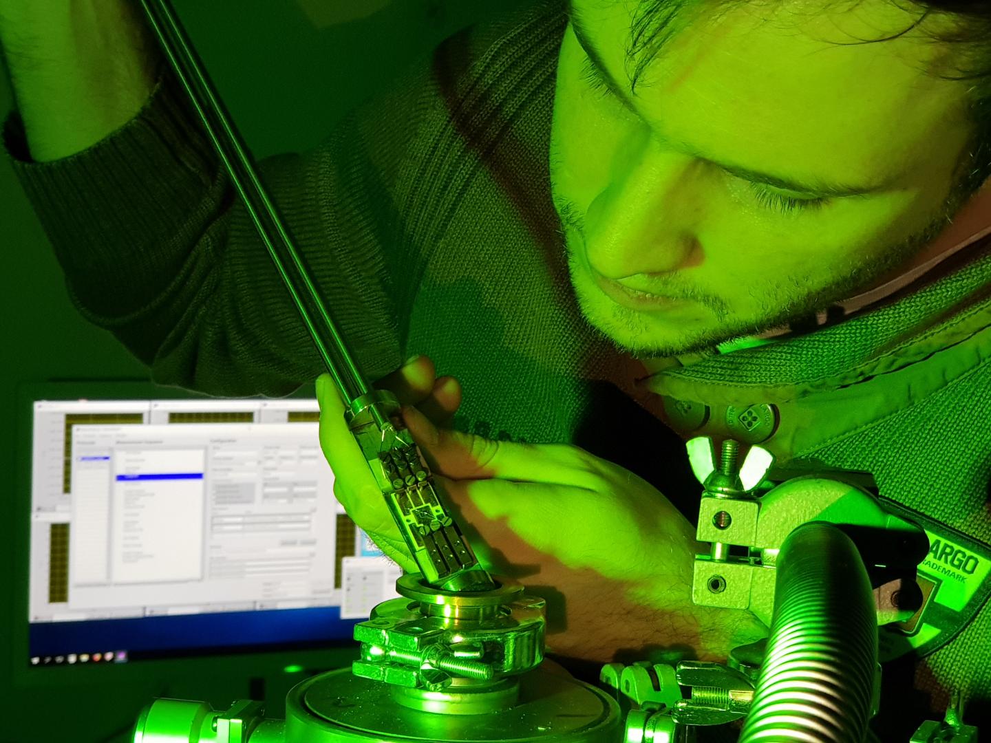
Researchers at Friedrich-Alexander-Universität Erlangen-Nürnberg (FAU) have developed a simple yet accurate method for finding defects in the latest generation of SiC transistors. This will speed up the process of developing more energy-efficient transistors in future. They have now published their findings in the journal Communications Physics.
SiC MOSFETs work on the basis of the interface between the SiC and a very thin layer of silicon oxide which is deposited or grown on it. It is this interface, however, which poses a significant challenge for researchers: during fabrication, undesired defects are created at the interface which trap charge carriers and reduce the electrical current in the device. Research into these defects is therefore of paramount importance if we are to make full use of the potential offered by the material.
Conventional measurement techniques, which have usually been developed with silicon MOSFET devices in mind, simply ignore the existence of such defects. Whilst there are other measurement techniques available, they are more complex and time-consuming, and are either unsuitable for use on a large scale or are simply not suitable for being used on finished components at all. This is the reason why researchers at FAU decided to focus on finding new, improved methods for investigating interface defects - and they were successful.
They noticed that the interface defects always follow the same pattern. 'We translated this pattern into a mathematical formula,' explains doctoral candidate Martin Hauck. 'Using the formula gives us a clever way of taking interface defects into account in our calculations. This doesn't only give us very precise values for typical device parameters like electron mobility or threshold voltage, it also lets us determine the distribution and density of interface defects almost on the side.
In experiments conducted using transistors specially designed for the purpose by the researchers' industrial partners Infineon Technologies Austria AG and its subsidiary Kompetenzzentrum für Automobil- & Industrie-Elektronik GmbH, the extremely simple method also proved to be highly accurate. Taking a close look at the inner core of the FETS allows now for improved and shorter innovation cycles. Using this method, processes aimed at reducing defects can be evaluated accurately, quickly and simply, and work at developing new, more energy-saving power electronics can be accelerated accordingly.
'An adapted method for analyzing 4H silicon carbide metal-oxide-semiconductor field-effect transistors' by Martin Hauck et al; Communications Physics volume 2, Article number: 5 (2019)


