
Improving The Performance Of Power Transistors
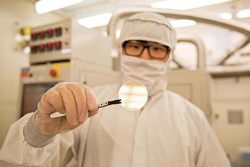
PHOTO: Vertical fin power FETs on a 2-inch GaN-on-GaN wafer.
Researchers at IEDM offers insights into how to make GaN transistors switch faster, produce higher blocking voltages, exhibit a very low on-resistance and completely supress dynamic on-resistance by Richard Stevenson
There is still much work to do to improve the performance of the GaN power transistor. While its commercialisation is netting sales, far greater revenues could follow if this device switches more efficiently, handles higher voltages and currents, and offers greater stability.
Options for succeeding on all these fronts were outlined at the recent International Electron Devices Meeting (IEDM), held in San Francisco from 2-6 December 2017. At that gathering researchers detailed: improvements in the switching performance of transistors that feature a gate insulator over the junction; the tremendous capability of vertical power transistors with fins and trenches; and the elimination of dynamic on-resistance through proton irradiation.
Speedier switching
A device architecture for providing superior switching was presented by Satoshi Nakazawa from Panasonic Corporation. Working with colleagues from Osaka University and Hokkaido University, he and his co-workers developed a GaN transistor with an AlON gate insulator that combines fast switching with a low leakage current.
"The proposed device exhibits a two-to-four times faster switching speed compared to a typical silicon super-junction-MOS with the same drain current rating," says Nakazawa. "This suggests a reduction in switching loss to half or less in high-frequency switching operations."

Figure 1. A team from Panasonic, Osaka University and Hokkaido University have developed a GaN transistor with an AlON gate insulator. This device combines fast switching with low leakage.
What's more, improvements wrought by the addition of the AlON gate should be applicable to all forms of GaN transistor, argues Nakazawa. "Those with a vertical architecture should expect similar results "“ such as stable gate characteristics with low gate leakages and a large gate voltage swing "“ ensuring gate-driving compatibility with conventional silicon power devices."
The team from Japan had to modify the standard HFET design to realise high-current, high-voltage switching. Their approach, introducing an insulator over the gate, has often been discussed as a way to to reduce leakage current and enable normally-off operation. However, success with this approach has not been reported prior to the work of Nakazawa and co-workers "“ instability of gate characteristics has probably hampered previous efforts.
Fabrication of the team's device (see Figure 1) began with growth, by MOCVD, of GaN and AlGaN layers on a silicon substrate (see Figure 2 for an overview of the fabrication process). Subsequent etching created a recessed gate structure, introduced to trim series resistance. After this, a thin AlGaN layer was added by MOCVD "“ this is highly beneficial, removing damage on the grooved structure caused by dry etching.
The next step involved adding AlON by atomic layer deposition, a growth process that combines great uniformity with an absence of processing damage. Annealing followed, to remove dangling bonds of gallium and/or aluminium at the AlGaN surface and ultimately ensure a positive shift of the threshold voltage. To realise a breakdown voltage in excess of 600 V, transistors were formed with a 2 μm gate length and a 10 μm gate-to-drain spacing.

Figure 2. The fabrication steps employed for the fabrication of a GaN transistor with an AlON gate insulator. This transistor is being pioneered by a team from Panasonic, Osaka University and Hokkaido University
Measurements of transfer characteristics reveal that the hysteresis of the team's annealed device is far less than that for a transistor with a gate made from Al2O3, a more conventional gate dielectric. The curves for transfer characteristics for the device with an AlON insulator do not change for gate voltages up to 10 V, leading Nakazawa and co-workers to claim that a high gate voltage can be applied to realise high-speed, on-state switching.
Further evidence for the benefits of AlON over Al2O3come from capacitance-voltage measurements. They show that dispersion is smaller for the novel oxide, and thus suggest a superior interface. Further encouraging signs come from values for interface trap densities, extracted from the capacitance-voltage measurements, that show that imperfections are lower for AlON, especially in the mid-gap.
Devices with a chip size of 2.3 mm by 2.3 mm are capable of a maximum drain current of 20 A, a breakdown of 730 V, and turn-on and turn-off transitions at 78 V/ns and 169 V/ns, respectively. "We are planning to demonstrate some practical applications," says Nakazawa. This will include converters formed with the team's devices.

Figure 3. Vertical fin power FETs are being developed by a partnership between researchers at MIT, the Singapore- MIT Alliance for Research and Technology, IQE RF and Colombia University. A key feature of these devices is that they don't require p-type material.
Fantastic fins
Supporting some US-based efforts at developing vertical GaN transistors with high-current, high-voltage capability is the ARPA-E SWITCHES programme. Working within this is a team involving researchers from MIT, the Singapore-MIT Alliance for Research and Technology, IQE RF and Colombia University. Together, they have produced vertical fin power FETs that combine an on-current in excess of 25 kA cm-2 with an off-current of less than 10-4 A at 1200 V.

Figure 4. Vertical fin power FETs produced by the team from MIT, the Singapore-MIT Alliance for Research and Technology, IQE RF and Colombia University produce a very competitive performance when compared to other vertical GaN transistors. The numbers in brackets refer to: [1] H. Nie et al. IEEE Electron Dev. Lett. 35 939 (2014) [2] D. Shibata et al. IEEE IEDM 10.1 (2016) [3] T. Oka et al. ISPSD 459 (2016) [4] M.Sun et al. IEEE Electron Dev. Lett. 38 509 (2017) [5] R. Chu et al. IEEE Electron Dev. Lett. 32 632 (2011) [6] C. Gupta et al. IEEE Electron Dev. Lett. 38 353 (2017) [7] M. Ishida et al. IEEE Trans. Electron Dev. 60 3053 (2013) [8] M. Wang et al. IEEE Trans. Electron Dev. 61 2035 (2013) [9] J. Ma et al. IEEE Electron Dev. Lett. 38 367 (2017)
In the paper given at the conference by Yuhao Zhang from MIT, it is stated that vertical devices have three key advantages over their lateral cousins: for a given chip area, a higher breakdown voltage and current; a superior reliability; and simplified thermal management.
However, according to the team, the majority of vertical architectures are held back by either the need to undertake an epitaxial re-growth step, or to have to grow p-type GaN. For devices such as current-aperture vertical electron transistors, epitaxial re-growth is essential, and it greatly increases the cost and complexity of device fabrication.
Meanwhile, p-type material is plagued by poor activation and a low carrier mobility. These impediments make it extremely difficult to produce a high-mobility intrinsic carrier channel, and they manifest themselves in a substantial increase in device on-resistance.
"Also, the need for p-GaN activation after MOCVD growth makes the overall wafer epitaxial growth complicated: on one hand, the thickness of p-GaN and the top layer is typically limited; on the other hand, the following growth of the top layer in MOCVD could easily passivate the p-GaN layer and make it n-type" argues Zhang.
With the approach he and his co-workers adopt, the need for p-type material is eliminated. "[Our devices] can achieve a normally-off operation without p-GaN , which is needed in many normally-off lateral HEMTs and vertical trench MOSFETs," says Zhang. "In addition, this threshold voltage can be well tuned by fin width, doping concentration and gate metal."
In the team's device, the current is controlled by fin-shaped, n-type GaN channels, which are surrounded by gate dielectrics and metal electrodes (see Figure 3). Due to the difference in the values of the work function for the gate metal and GaN, the electrons in the fin channels are depleted at zero gate bias. Once the fin width is reduced below 500 nm, the depletion regions induced by the two free surfaces of the fin merge to form a fully depleted fin channel that enables normally-off operation.
Back in April 2017, the team reported an early form of their device, which combined a blocking voltage of 800 V with an on-resistance of 0.36 mΩ cm2. Since then they have improved the device, with the latest results reported at IEDM.
Zhang says that the recent device benefits from refinements to the wafer structure, especially engineering the doping level and thickness of the drift region "“ this can lead to a better trade-off between on-state conductivity and off-state breakdown capability. The process for making ohmic contacts has also moved on, allowing "excellent" ohmic contacts to be formed on top of the narrow fins, even without the need for post-annealing. What's more, the team has refined the design so that the peak electric field has shifted from the fin to the device periphery. "This makes electric field management much easier," says Zhang.
Fabrication of the transistors began by taking free-standing GaN substrates and growing, by MOCVD, a 2 μm-thick n-type layer, followed by a 7 μm-thick n-type GaN drift layer that is doped with carbon to compensate the non-intentional doping in GaN, and finally a 300 nm-thick n-type GaN cap.
Fins were formed by dry-etching, before additional structures were formed between and on top of the fins, using plamsa-enhanced CVD of SiO2 spacer layers, atomic layer deposition of an Al2O3 gate dielectric, and sputtering of a molybdenum gate layer.
Measurements on a device with 60 fins, each with a width of 200 nm and a length of 100 μm, revealed a threshold voltage of about 1 V, an on-off ratio for current of 1010, and an on-resistance of 0.2 mΩ cm2. Breakdown voltage exceeded 1200 V, and drain and gate currents were below 1 nA at high drain bias.
Zhang and co-workers also produced a larger device with a 10 A current rating. Featuring 600 fins with widths of 250 nm, this chip required a gate drive of 5-6 V to produce 10 A, and had a breakdown voltage of 800 V. The team claims that this chip, which is 0.8 mm by 0.55 mm in size, is significantly smaller than other 10 A-class GaN vertical and lateral transistors.
Benchmarking of the team's devices against those of other groups underlines the impressive performance of the vertical fin power FET (see Figure 4). And even better results are sure to follow.

Figure 5. A team from the University of California, Davis, and the University of California, Santa Barbara, is developing oxide-GaN interlayer FETs under support from the ARPA-SWITCHES programme. These FETs, which can deliver blocking voltages in excess of 1.4 kV, feature trenches and double field plates.
"We have already made devices capable of sustaining 2000 V reverse bias," says Zhang. "We are now incorporating additional edge termination structures to achieve even higher breakdown voltage uniformly on a wafer-level."
The researchers from MIT are also collaborating with IBM and Columbia University, with the aims of accomplishing wafer-level device transfer and providing circuit demonstration. "The goal is to recycle the expensive GaN substrate, to greatly reduce the cost of the power modules built from our novel vertical GaN transistors," explains Zhang.
Vertical trenches
The ARPA-SWITCHES programme is also supporting a team from the University of California, Davis, and the University of California, Santa Barbara. This partnership is pioneering the development of oxide-GaN interlayer FETs. Unit devices are capable of blocking voltages of more than 1.4 kV, while the figure for large-area devices is 900 V. Spokesperson at IEDM meeting, Dong Ji from the University of California, Davis, says that they are pursuing this device architecture, rather than the current aperture vertical electron transistor, because although the latter is capable of a high current density, it is a normally-off device. Another alternative, the trench MOSFET, has a good normally-off behaviour, but it has been shunned, due to its a low current density that stems from the low channel electron mobility.
"The novelty in an oxide-GaN interlayer FET lies in using a ten-nanometre, MOCVD-regrown unintentional doped GaN interlayer as the channel region, which improves the channel electron mobility without hurting the normally off behaviour," says Ji.
According to him, the team's device, which has a channel mobility of 185 cm2 V-1 s-1, has the highest mobility of any reported oxide-based GaN or SiC power transistor.
"For the conventional GaN trench MOSFET and SiC trench MOSFET, the channel electron mobility is limited to 50 cm2 V-1 s-1, which is limited by the high doping density in the p-base region," says Ji. "However, because the oxide-GaN interlayer FET uses unintentionally doped GaN as the channel, the channel mobility is improved."
Devices were formed by taking epiwafers, grown by IQE, and etching 550 nm deep trenches. Following a clean with HF acid, MOCVD added a 10 nm-thick, unintentional grown GaN layer, followed by a 50 nm-thick layer of Al2O3. These two layers serve as the channel and gate insulator, respectively. The addition of source, gate and drain electrodes and field plates completed FET fabrication.
"We used a double field plate structure," says Ji, who explains that one of the field plates is connected to the gate contact, and the other to the source contact. "Compared to the single field-plate structure, which protects the source-to-drain p-n junction, the double-field-plate structure can protect the gate insulator to improve the breakdown voltage, and improve the gate insulator reliability."
Measurements on single unit cell devices, which have a circle layout with a 22 μm diameter, reveal a saturated current density of 850 A cm-2, an on-resistance of 2.2 mΩ cm2, a breakdown voltage of 1435 V and a threshold voltage of 4.7 V.
"4.7 V is an excellent value for power devices," says Ji, who attributes this success to the doping density in the GaN interlayer.
The team also produced larger transistors, with an area of 400 μm by 500 μm. These devices produce a breakdown voltage of 900 V and a saturation current of 0.185 A under a 12 V gate bias.
Ji says that the next steps will be to demonstrate a single device with a current of more than 10 A, and to study its switching characteristics. "Commercialization of the device is our goal." All the fabrication steps are commercially viable, argues Ji, pointing out that all growth steps can be undertaken with MOCVD, which is preferred for mass production.
Proton perfection
One of the weaknesses of the GaN transistor is its dynamic on-resistance. This downside can result in an increase in total on-resistance of up to 30 percent, following exposure to a high drain bias.
At IEDM, Matteo Meneghini from the University of Padova, Italy, outlined an approach for completely eliminating dynamic on-resistance: proton irradiation. Working with departmental colleagues, as well as researchers from ON Semiconductor, he has shown that GaN HEMTs can undergo complete suppression of the dynamic on-resistance over the voltage range of 0 V to 600 V when given an optimal dose of protons.
Meneghini says that dynamic on-resistance is strongly dependent on the leakage through the unintentionally doped layer. However, eliminating leakage by improving the growth of this layer is very challenging, making proton bombardment a more practical approach.
The time taken to carry out the irradiation of protons is "short", say Meneghini, and depends on the fluence.
Experiments by the team, using conventional devices, show that there is no change in the dynamical behaviour for fluences of 1012 cm-2 and below.Increase the fluence to 1013 cm-2 and there is a slight reduction in dynamic on-resistance; and this reduction is substantial for a fluence of 5 x 1013 cm-2 and completely suppressed when the fluence is 1.5 x 1014 cm-2 (see Figure 6).
Meneghini believes that proton irradiation could be used during the manufacture of GaN transistors. He points out that irradiation/implantation is used in the optoelectronics industry to create highly resistive regions in laser diodes.
Work on this topic will continue, with Meneghini and co-workers aiming to study and optimise treatment conditions, investigate the impact of different epitaxial processes, and study the trade-off between leakage and dynamic on-resistance.
These efforts, along with further progress from the teams working in the ARPA SWITCHES program and for Panasonic, will help to improve the performance and capability of GaN transistors. Reports of more breakthroughs in this field can be expected at this year's IEDM, which will be held in San Francisco from 3-5 December.


