

Removing GaN from GaN
Photoenhanced wet etching of InGaN leads to lift-off of high-quality heterostructures by Chris Youtsey and Robert McCarthy from Microlink Devices and Andy Xie from Qorvo
In the early days of the compound semiconductor industry, device production involved the growth of lattice-matched epilayers on GaAs and InP substrates. Now the range of materials has expanded to include GaN, which may be grown on mismatched substrates such as sapphire, SiC and silicon.
For all these material systems, the substrate plays an essential role in the growth process, serving as a crystalline template for building up a device structure, layer by layer. But once the growth is complete, the substrate is merely an expensive handle. It can even be suboptimal, with the device delivering a better performance "“ such as superior light extraction, reduced weight, enhanced thermal conductivity or increased flexibility "“ when its layers are transferred intact to a new, better handle.
One way to enjoy these benefits is to mechanically thin the substrate. However, that's not ideal, as it's a destructive process. Better is the use of an epitaxial lift-off (ELO) process, as this does not damage the substrate during the removal of the epilayers. This technique uses a sacrificial release layer that is selectively etched to separate the epitaxial layers from the substrate. By taking this approach, it is possible to reuse the substrate many times, promising considerable cost savings.
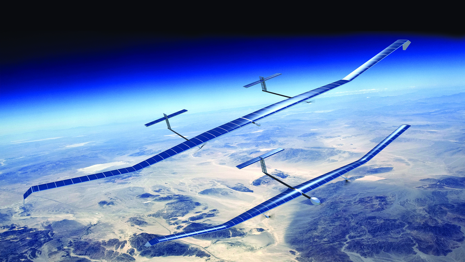
For the past ten years our team at Microlink of Niles, IL, has been pursuing this approach by developing an ELO technology for compound semiconductor materials. Our successes during that time have led to the use of ELO in the volume manufacture of inverted metamorphic multi-junction solar cells with a 6-inch diameter. These cells combine an exceptionally high efficiency of more than 30 percent in AM0 conditions with a specific power exceeding 3000 W/kg. The removal of the substrate holds the key to such a high specific power, and it also trims costs through its re-use. The very high efficiencies and specific powers of our cells make them strong candidates for serving the emerging market of high-altitude, long-endurance unmanned aerial vehicles. With this solar technology, flights can last for weeks and even months.
We are now breaking new ground by extending the capability of our technology so that it can be applied to GaN. In this material system we have pioneered the development of a relatively fast wafer-scale photochemical lift-off process that does not have to draw on an exotic material for the release layer "“ instead, it uses InGaN.
Figure 1. A flexible solar array fabricated using MicroLink ELO multi-junction solar cells (left). High-altitude long-endurance (HALE) aircraft such as the Airbus Zephyr require very lightweight, high-specific-power solar cells enabled by MicroLink's ELO technology (main image).
GaN: Opportunities and challenges
To date, foreign substrates have not hindered the commercial progress of GaN devices, which are second only to silicon in market size. Thanks to the success of LEDs and HEMTs grown on sapphire, silicon and SiC "“ all these devices perform remarkably well, considering their high dislocation densities that stem from the use of mismatched substrates.
However, despite this success, epitaxial lift-off and layer transfer processes can be a major asset for GaN devices, improving their performance through the use of a native substrate. Many would agree that the widespread availability of high-quality, low-cost GaN heterostructures, grown on native GaN substrates, can lead to a new generation of transformative power devices. They include vertical GaN devices, such as vertical-junction FETs and HBTs, that need low dislocation densities to realise high current densities. Compared with the conventional silicon power devices, these power switches, which are based on vertical GaN architectures, will deliver a far lower on-resistance and a much higher operating frequency. These strengths will propel efficiency to new highs.
Figure 2. The ELO process begins with an epitaxial structure that has a sacrificial release layer between the substrate and device layers. A flexible carrier is attached to the top of the device layers, and wet chemical etching dissolves the release layer to achieve lift-off.
With GaN-on-GaN device technology, epitaxial lift-off is highly synergistic. The primary motivation is economic; GaN substrates are inherently expensive, and substrate reuse after the ELO process promises to slash substrate costs.
However, just as important as the cost savings is the ability to transfer the device to a substrate with superior thermal characteristics. That's because the performance of a high-power GaN-on-GaN device is then limited by the thermal conductivity of the native GaN substrate. The improved thermal performance that results from layer transfer can enable either an increase in power densities or a trimming of die size. According to our modelling, when a GaN vertical-junction FET is fabricated with an ELO process, this improvement can trim the chip size by more than 50 percent.
In addition to the benefits associated with the use of ELO from native GaN substrates, this technology can separate an LED from its sapphire substrate. This step, which increases light extraction, is normally accomplished by laser lift-off. A high-power laser is rastered over the wafer, vaporising the interface between GaN and sapphire. With our ELO process, there is far less damage at the interface, and lift-off can take place at the wafer scale.
Realising release
With any ELO process, the central challenge is to identify a suitable material for the release layer. This layer is inserted between the substrate and the active layers of the device, and sacrificially removed using wet chemical etching, to enable lift-off.
Figure 3. GaN is resistant to conventional wet etchants, but ultraviolet illumination can enable rapid photoenhanced wet etching. On the left is shown a cross-shaped feature, etched 5 μm deep by photoenhanced wet etching using a titanium metal etch mask. Under certain conditions, the etch process can be highly selective to material defects. The image on the right shows threading dislocations, revealed as "˜whiskers' formed by photoenhanced wet etching of a GaN-on-SiC structure. Reproduced from C. Youtsey et al. Appl. Phys. Lett. 71 2151 (1997) and C. Youtsey et al. Appl. Phys. Lett. 74 3537 (1999)
The release layer must fulfil several key requirements: it must be etched with high selectivity to prevent damage to the surrounding substrate and device layers; it must have a high enough lateral etch rate to ensure that it does not take too long for large areas to be released; and its insertion must not degrade the quality of the material grown on top of it.
Applying ELO to GaAs materials is relatively easy. In this case, AlAs and InGaP can be used as lattice-matched release layers, which can be etched with a very high selectivity relative to GaAs. With GaN, however, the situation is far more tricky, because the usual rules do not apply to nitride materials.
Figure 4. MicoLink's approach to ELO of GaN is based on bandgap-selective, photoenhanced wet etching using an InGaN release layer. Filtered UV illumination is transmitted through the backside of the GaN substrate and absorbed in the InGaN release layer (shown in yellow), driving selective etching of that layer. The frontside of the wafer is metallized and patterned with perforations to accelerate the ELO process. Reproduced from C. Youtsey et al. Phys. Status Solidi b, 10.1002/pssb.201600774, (2017)
After we grow the full epitaxial device structure, including the release layer, we add a thick metal support layer to the topside of the wafer. This metal layer provides mechanical support to the GaN film after it has been fully released, as well as electrical contact to the GaN. During the etch process, electrons are conducted from the metal support layer to the platinum counter electrode in the potassium hydroxide etch solution. The metal layer is patterned with cross-shaped perforations (see Figure 6), typically on a 1-4 mm pitch. The perforations accelerate the removal of large, wafer-scale films by enabling etching to occur from many locations across the wafer. Photoenhanced wet or dry etching transfers the perforation patterns through the entire epi structure and into the bulk GaN, to enable access of the etching solution to the buried release layer (such structures are shown in Figure 4). If our device structure contains InGaN layers with a similar indium composition to the release layer, we modify our process "“ prior to etching, we passivate the sidewall of the etched via hole with a dielectric layer. This prevents unintentional etching of the device layers during the ELO process. 
Thanks to the optical transparency of the GaN substrate, the ELO process can be seen in real time (see Figure 7, which shows a sequence of images). After one hour there is material still to be etched "“ it is visible as dark diamonds, at the centre of each 1 mm x 1 mm unit cell "“ but after two hours the film has been fully released. While etching is relatively slow compared to other device fabrication steps, the ELO process is low cost, and can be performed in large batches to achieve high throughput.
Figure 5. A cross-sectional, scanning transmission electron microscopy image of a GaN-on-GaN ELO epitaxial structure with an InGaN release layer. The interface between the GaN substrate and epitaxial layers is shown with a red dashed line. The material grown above the release layer is free of defects and has high-quality interfaces. Reproduced from C. Youtsey et al. Phys. Status Solidi b, 10.1002/pssb.201600774, (2017)
We have used our ELO technology to completely remove a 4-inch GaN epitaxial layer from a 4-inch sapphire substrate (see Figure 8). The film of GaN, just 5 μm-thick, is supported by the metal backing layer.
Our ultimate objective is to realise the lift-off of GaN films from native GaN substrates. This has been accomplished, using 2-inch GaN substrates made by the SCIOCS Company Limited and Sumitomo Electric, Inc, using cross-shaped perforations with a 1 mm pitch (see Figure 9).
Device demonstration

Figure 6. After growth of the GaN epitaxial structure, a metal support layer is applied to the top of the wafer. Cross-shaped perforations, patterned in the metal layer, are etched through the epi structure down to the release layer, as shown in the top scanning electron microscopy image. The high-magnification image on the bottom shows the vertical sidewall of the etched perforation, with the release layer interface clearly visible. Reproduced from C. Youtsey et al. Phys. Status Solidi b, 10.1002/pssb.201600774, (2017)
Following our demonstration of the capability of ELO to remove full-wafer films of GaN, we have gone on to validate the quality of the lifted-off GaN material through the fabrication and testing of devices in Patrick Fay's research group at the University of Notre Dame. This effort began with the fabrication of planar Schottky diodes on GaN-on-sapphire structures (see Figure 10). 
Figure 7. The lateral etching of the release layer during the ELO process can be directly observed through the transparent GaN substrate. Shown are images taken after zero, one and two hours of etching. The film has partially released after one hour (the dark regions at the centre of each unit cell are unetched), and has completely lifted off after two hours. Reproduced from C. Youtsey et al. Phys. Status Solidi b, 10.1002/pssb.201600774, (2017)
Reverse-bias current-voltage plots on a diode before and after the ELO process show a fall in leakage after lift-off of more than an order of magnitude (see Figure 10). Results were obtained by fabricating and testing the diode on the original substrate, and then encapsulating it with metal, applying the lift-off process, bonding the device to a new carrier using an insulating adhesive, and then retesting it after the removal of the metal support layer. 
Figure 8. Shown is a GaN film fully released from a 4-inch sapphire substrate, supported by the frontside metallization. Under UV illumination the GaN material luminesces bright yellow-green, as seen on the right. Reproduced from C. Youtsey et al. Phys. Status Solidi b, 10.1002/pssb.201600774, (2017)
Dislocations in the device account for the dramatic reduction in the reverse-bias leakage current after ELO and layer transfer. The dislocations are prevalent, due to growth on sapphire, with vertical dislocations intersecting both the ohmic and Schottky contact pads (as illustrated in Figure 11). As these dislocations can be conductive, high-power vertical GaN devices must have a low dislocation density to work well. That's not the case prior to the ELO process, due to a conductive path that threads between the Schottky and ohmic contact pads, and laterally through the n+ GaN layer beneath the release layer. The lateral current path through the n+ GaN layer is eliminated after ELO. Leakage is then far lower, thanks to the bonding of the device to an insulating carrier.
We have also fabricated and tested p-n junction diodes, using GaN-on-GaN structures. These devices, which have a planar contact structure that is similar to that for the Schottky diodes, produce a very similar reverse leakage current before and after the ELO process (see Figure 12). This is not surprising, given that the dislocation density in the bulk GaN substrates is in the range of 106 cm-2, which is at least three orders of magnitude lower than that for GaN-on-sapphire. No defect-related leakage current mechanisms were observed in these diodes.
Figure 10. Current-voltage (I-V) curves for GaN-on-sapphire Schottky diodes measured before lift-off (blue curve) and after lift-off (red curve). The diodes feature a square Schottky contact in the centre and an annular ohmic contact around the perimeter. Permission for reproduction granted by IEEE. Reproduced from J. Wang et al. in: Proceedings 74th Annual Device Research Conference (DRC), Newark, DE, 2016, pp: 1 "“ 2.
From now on we will focus on optimising the bulk GaN substrate reclaim process, and establishing how many times a substrate can be reused. Working in collaboration with Sumitomo Electric, Incorporated, we have already successfully reclaimed a bulk GaN substrate after ELO. Results will be published shortly. Our initial estimates indicate that a substrate can be reused at least five to ten times. If that's the case, this will slash the effective substrate cost.
Figure 11. Dislocations provide a vertical current path for leakage between the Schottky and ohmic contacts, with a lateral current path through the n+ GaN layer beneath the release layer (shown near right). After ELO, the lateral current path has been removed, leading to the reduced leakage current (far right). This illustrates the importance of low-dislocation density bulk GaN for vertical power devices. Permission for reproduction granted by IEEE. Reproduced from J. Wang et al. in: Proceedings 74th Annual Device Research Conference (DRC), Newark, DE, 2016, pp: 1 "“ 2.
Another of our goals is to develop effective methods for bonding lifted-off films to new substrates with high thermal conductivity. These new processes will be integral to a GaN ELO technology that has the potential to substantially improve the economics and performance of GaN-on-GaN power and optoelectronic devices.
The authors are grateful for support provided by the ARPA-E SWITCHES program under grant number DE-AR0000446 (program managers Tim Heidel and Isik Kizilyalli). We'd also like to acknowledge the work of our team members. GaN epitaxial layer structures in this project were grown by Andy Xie and Ed Beam at Qorvo, Inc., and Professor Louis Guido at Virginia Tech. Device fabrication and testing was carried out at the University of Notre Dame by Jingshan Wang and Professor Patrick Fay. Rekha Reddy at MicroLink Devices developed GaN layer transfer and bonding processes.
Figure 12. Current-voltage (I-V) curves for GaN p-n diodes grown on bulk GaN substrates, measured before and after epitaxial lift-off. No change in device performance was observed during the layer transfer process. Reproduced from C. Youtsey et al., in: Proceedings CSMANTECH Conference, Indian Wells, CA, 2017


