Effective hermetic sealing for next-generation microelectronic packaging
A perfectly sealed electronic package can fulfill its intended function
without disruption, error or a significant reduction in performance for
decades. However, design and field engineers can only achieve this level
of performance by applying the right materials and sealants, and
employing the correct tools, equipment and process steps to build
semiconductor-driven electronic packages for the next generation. The
confidence engendered by a well-sealed package inevitably leads to the
development of better chips with more features.
BY RAMESH KOTHANDAPANI, TECHNICAL DIRECTOR, MICROELECTRONIC PACKAGING, MATERION CORPORATION
HERMETIC SEALING is an important process for packaging semiconductor chips. The word “hermetic,” in this case, suggests leak-safe sealing. A semiconductor chip goes through several process steps, starting as a wafer before being cut into individual chips and eventually ending up in a discrete package. Such chips are strongly bonded to die pads with a die-attach epoxy or eutectic solders. They are then electrically connected to the ceramic package bond pads with very fine wires.
The ceramic package – in effect a “chip carrier” – is generally multi-layered with electrical feedthroughs within its ceramic body. These layers are internally connected to the bottom or sides of the package to be mounted onto printed circuit boards along with other electrical components. An array of packages is available for chip bonding, including leaded chip carrier (LCC); ceramic, quad, flatpack (CQFP), and quad-flat package (QFP), among others.

The ceramic package is seam-sealed with two electrodes running parallel to melt the lid and seal it to the ceramic or metal package.

The ceramic package with seal ring and wire and die-bond pads.

The ceramic package with chip attachment.

Ceramic package with seal ring dimensions.
The ceramic package containing the chip with wire bonds must eventually be hermetically sealed to prevent the entry of contaminants such as moisture or loose particles.
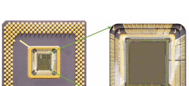
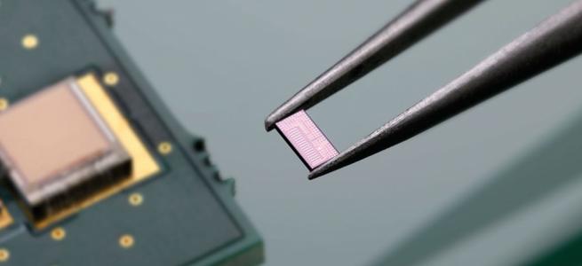
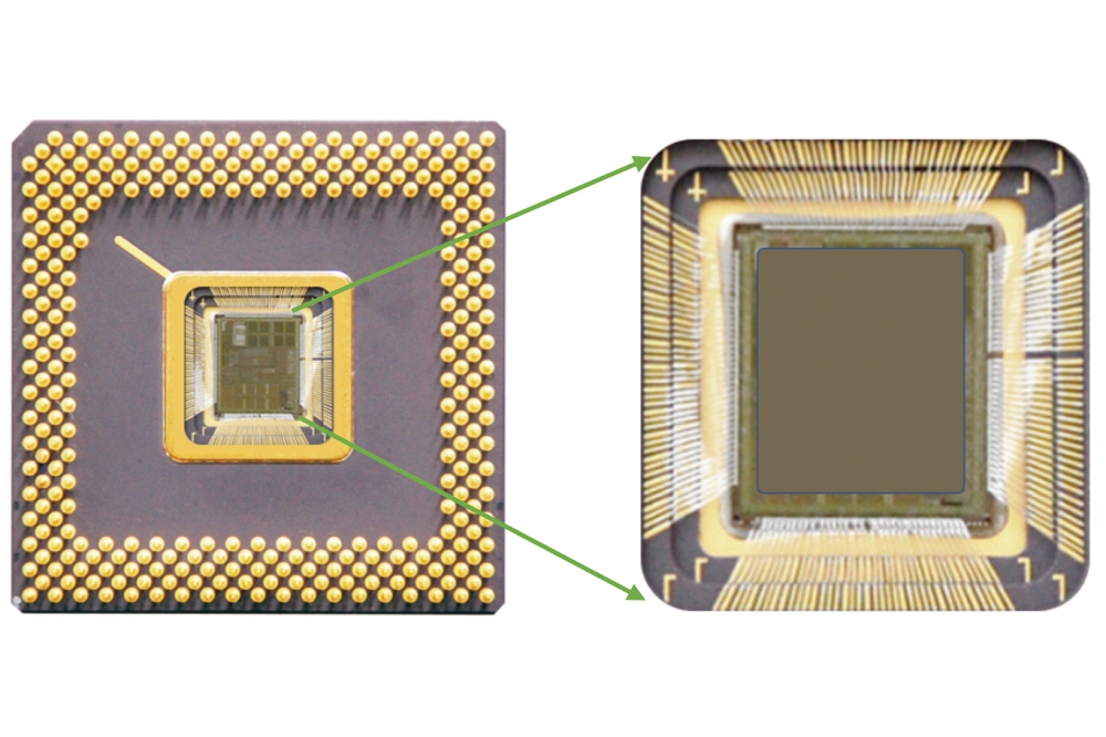
The hermetic sealing process is vital to determining the viability of the assembly in operation. Illustration 1 shows the semiconductor chip and its hundreds of very fine wire bonds. These chips range in size from a few millimeters to tens of millimeters. Smaller chips may have fewer wire bonds, while larger chips can have hundreds. These bonds are thinner than a human hair, with diameters as small as 0.0007 inch (17.78 microns).

Design guidelines for package lid and solder.

Illustration 7. Gold-Tin phase diagram.

Exploded view of ceramic package, solder frame and plated metal lid.
Discrete chips contain micro-electromechanical systems (MEMS) with super-fine gears, clocks and moving actuators that cannot be seen with the naked eye. Any particles that deposit on these chips are likely to interfere with their performance. Equally, with the bonded fine wires so close to each other, conductive particles or moisture between the wires could cause a malfunction. This makes proper hermetic sealing of the assembled packages even more important.
Before focusing on the sealing process, it’s important to know about materials which are used for sealings, its limitations, the design guidelines, storage, and handling processes.

Cross section image of four layers plated sequentially with nickel and gold.
There are, for example, several types of ceramic packages:
• Surface mount ceramic packages
• Ceramic pin grid array packages
• Ceramic quad flat packages
• Ceramic hybrid packages
• Fiber-optic communication packages
• The bonding materials or solders
• The components which have to be attached to the package such as dies, die attach materials, wires and etc.
Depending on the level of hermeticity required, packages undergo one or two sealing processes: seam-sealed with a metal lid, or solder-sealed with a plated metal lid.

Nickel migration process.

Frame lid assembly.

Tack weld points at corners.
SEAM-SEALED WITH METAL LID:
This is a reliable hermetic sealing process in which a pair of round electrodes run around the edge of the lid, melting and fusing it to the package’s seal ring area. Seam sealing is useful when:
• The semiconductor chip cannot accept high levels of heat. Seam seal offers localized edge heating.
• The user may not have oven reflow capability.
• The end application is RF-related with a low level of hermeticity required (i.e., RF packaging).
SOLDER-SEALED WITH PLATED METAL LID:
This process can also achieve high levels of reliable, airtight sealing. Several post-seal tests are available to confirm its effectiveness.
Some factors are common to all package types, including the use of die-bond pads, wire bond pads and seal rings. Illustration 3 shows some key features of the ceramic package.

Illustration 13. Critical parameter controls and recommendations for effective hermetic sealing using a belt furnace.
DIE-ATTACH PAD: This is the area where the semiconductor chip is attached with the aid of eutectic solder alloy or epoxy materials. Epoxy-based die-attach adhesives typically comprise a resin and a hardener, which must be well mixed before being applied to the die pad. The chip is then put into place and scrubbed with pressure to initiate wetting and release any trapped gasses in the bonding materials. The assembly is cured at high temperatures to harden it, a potentially tricky process that must be properly controlled.
Both 88Au12Ge and 80Au20Sn can be used as eutectic bonding materials. They melt at 361°C and 280°C, respectively. After considering the heat loss into the fixtures and other components, the set temperature is usually higher. Both types of eutectic solders are pure alloys without any binders or bonding agents.
The selection of the die-attachment bonding material is subject to the coefficient of thermal expansion (CTE) of the chip and other neighboring materials with which the bonding agent may come into contact. Melting and curing temperatures and conditions must also be determined.

Vacuum furnace inner chamber.
CHIP ATTACH POST-SEAL CONDITIONS:
It is important to validate secure bonding and ensure the release of trapped gasses. Suppliers will generally provide curing instructions and process steps to remove organics and binders. Otherwise, hydrogen-saturated hydrocarbons or moisture could release during the solder hermetic sealing process. Trapped gases within the package will negatively affect its overall electrical performance and lifespan.
Consequently, a well-controlled die-attach process is important for achieving void-free bonding. Unfortunately, post-seal validation can be costly and may produce irregular or misleading results. Close attention must be paid, then, to storage conditions, expiry date, mixing ratio, duration of use, and volume required per unit per shift. There is also the looming possibility of moisture absorbed from the environment.

Gold-tin reflow profile.
SEAL RING:
This is one of the most important components in the ceramic package when it comes to hermetic sealing. As is the case with die and wire bond pads, nearly the full surface of the seal ring is used in the soldering process. The seal ring surface is generally porous and plated with nickel and gold, which could lead to nickel migration to the seal ring at elevated temperatures. This in turn may result in pin holes and solder voids. Thus, careful handling and temperature control are essential.
Effective hermetic sealing: Step-by-step
Successful hermetic sealing is dependent upon several factors, including:
• Design guidelines for the package seal ring
• Sealant and lid material selection
• Sealing methods and process controls
• Post-hermetic sealing tests and troubleshooting
• Next-generation packaging material options
DESIGN GUIDELINES OF THE PACKAGE SEAL RING:
Consider the size of the hermetic cover lid and its solder. The outer seal ring, the metal lid, and the gold-tin frame are key design elements. For example, if the package seal ring outer length and width is 0.500” square, the lid should 0.500 inch - 0.010” - 0.010”, or 0.480” square.
Next is to determine the gold-tin solder inner dimensions. For this, both inner and outer dimensions must be considered. If the seal ring inner dimensions are 0.400” square, then the gold-tin solder inner dimensions should be 0.400” + 0.010” + 0.010”, or 0.420” square. The inner and outer radii are also important for the overall design, as is the thickness of the solder and lid. These dimensions will be based upon the size of the final package. The 0.010” clearance relies on the availability of space for the seal ring. It can be as low as 0.002” for the outer gap, and almost as low for the inner seal ring if the ring is narrow.

llustration 16: Left, assembly with pressure applied. Right, post-seal with solder fillet.
SEALANT MATERIAL SELECTION:
There is a variety of suitable solder alloys and eutectic solders for leak-safe hermetic joints. Gold-tin has been proven particularly effective for bonding metal lids to ceramic or metal packages. The 80% gold/20% tin solder melts at 280°C and holds up well when subjected to temperature cycle testing.
The 80% gold/20% tin alloy must be manufactured with very few impurities and must be within its nominal weight percentage to achieve a good bond.
• Gold-tin purity: Decrease in heat conductivity
• Gold-tin contamination: Oxides, organics
• Gold-tin interfacial contact area

Various reliability tests.
COVER LID MATERIAL SELECTION:
The metal lid is an alloy of iron, nickel and cobalt, also known as ASTM F-15. In order for the gold-tin solder to bond well with the package, the metal lid must be well prepared. A lid composed of more than 50% iron (Fe) elements could oxidize over time. A bare lid will not allow gold-tin solder wetting. Reliable gold plating is therefore essential.
The lid is electroplated with 100 to 350 microinches of nickel, followed by gold at a thickness of 50 microinches. Additional nickel and gold are plated for high-reliability applications, though the sum of both nickel films cannot exceed 450 microinches, while the sum of the gold-plated films must be at least 50 microinches. The idea is to prevent excess build-up at the edges. which could eventually have a negative effect on the hermetic seal. The following illustration shows a cross-section of the four-layer plated lid.
EFFECTIVE PLATING:
The plating process is extremely critical. Edge build-up, for example, must be avoided. The electroplate bath and chemistry maintenance are both important. It should be noted that this plating is not cosmetic in nature, but is rather designed for high-quality hermetic sealing, which also entails good solder bonding. Poor maintenance plating could trap unwanted gases.
Post-plate tests are available to check the quality of the plating, particularly to quantify hydrogen content in the plated films.
Plating bath maintenance and bath chemistry checks should be performed periodically for preventative reasons. Post-plate bakeouts are also sometimes performed following last-stage plating at lower temperatures (between 120°C to 150°C) for 8 to 12 hours.
High-temperature bakeouts for longer durations could cause the inner layer of nickel to migrate to the gold layer and interfere with solder wetting. The gold-tin solder alloy will not wet with nickel. Nickel migration may also occur if the plated layer is too thin or demonstrates high porosity on the plated surface.
Sealing methods and process controls
• Tack Welding or Spot Welding: The gold-tin solder must be attached to the plated lid by spot or tack welding. This process is crucial to avoiding misalignment and other defects that could eventually affect seal yield. It also creates
additional benefits for end users who must assemble the frame and lid as a single component before final sealing. Tack welding requires very small portions of the eutectic gold- tin solder at all four corners to melt and adhere to the plated lid.
• Reflow equipment and process controls: It’s important to select the proper reflow equipment prior to sealing. Hermetic sealing with gold-tin or other solders requires an inert environment; otherwise, oxidation might affect the integrity of
the seal. If a belt furnace is used, the maintenance and seal profiles must be well monitored. Oxygen content within the reflow chamber should be tracked and controlled. Similar monitoring is required if a vacuum seal furnace is chosen, with the additional benefit of removing unwanted gasses. In both cases, equipment performance will ultimately determine the quality of the hermetic seal.
The gold-tin seal profile: Following are key considerations for the gold-tin seal profile:
• Rise rate: The rise rate must be gradual and slow. This helps to release gasses from the various components without promoting nickel migration. Such migration may result from a quicker ramp-up, especially with porous-plated layers. Vacuum furnaces will evacuate any outgasses, while a belt furnace with nitrogen pressure should do the same.
• Peak temperature: Eutectic gold-tin solder melting temperature is 280°C. In addition to the sealing components, fixtures, clips and other materials can also pull in heat. Once the solder and lid reach peak temperature, the goal should
be the complete removal of gases, complete solder flowing, solder fillet formation, and the elimination of pin holes or void removal. Duration of exposure to peak temperature is very subjective and depends on product size, ssembly tools and conditions. Reducing this duration while critical processes are in progress can uncover failure modes, which can be observed visually, through leak tests or under X-ray.
• Ramp down from peak zone: Product cooling must also be done gradually, as sudden cooling or ejection of the product from the oven can be quite harmful.
• Adequate pressure should be applied to gold-tin solder to achieve a good hermetic joint. Interestingly, though, only about 0.5 to 4 kilogram-force is required. In all cases the pressure is transferred from the lid down to the gold-tin sealant (see Illustration 16). As mentioned, this pressure is very helpful during the peak temperature phase to press the lids and squeeze out molten solder to form a fillet.
SEAL CLIPS:
There are many different types of readily procurable clips. Depending on the type of package and production volume, pressure clips can be customized and fabricated. The aligning fixture should also be considered if increased production volume is desired.
POST-SEAL RELIABILITY TEST:
Post-seal reliability tests validate process and material selection. Several different levels of tests are performed one after another. Details of all listed tests can be found in standard Mil-883 guidebooks.
NEXT-GENERAL PACKAGING MATERIAL OPTIONS: These tests are intended to confirm successful hermetic sealing. Similarly, an effective packaging process can significantly prolong the life of the package in field. Many applications, such as a board-level module installed in a satellite or space vehicle, are not reachable for replacement or repair. Thus, they are made to last even in the most adverse conditions.
A variety of new materials and processes are coming into the market. For next-generation hermetic sealing applications, for example, a range of innovative cover lids are now available. These include hermetic covers or Visi-Lids for optical communications, non-magnetic Combo Lids for electromagnetic nose controls, and Getter Combo Lids to contain the release of hydrogen from the package.