ADC ‘breakthrough’ highlights power efficiency innovations
Imec research developments featured at the recent International Solid-State Circuits Conference (ISSCC) 2024, included a massively time-interleaved slope-ADC prototype chip demonstrating ‘superior scalability’ to meet data centers’ exploding bandwidth and data processing demands; a novel ultrasound-powering technology paving the way to miniaturised and minimally invasive neural implants; and a low-power, ultra-Wideband (UWB) receiver chip said to be ten times more resilient against interference from Wi-Fi and (beyond) 5G signals.
IMEC INTRODUCED a breakthrough architecture that lays the foundation for a whole new generation of analog-to-digital converters (ADCs). Imec’s massively time-interleaved slope-ADC design offers high power efficiency and a very compact footprint, while promising to enable exceptional conversion speeds. As such, it is ideally suited to meet data centers’ exploding data processing and throughput demands, driven by the surge in cloud computing and (generative) AI applications.
Training AI models requires massive computing power, necessitating data centers to invest in increasingly powerful optical networks for fast, reliable communications between servers, storage devices, and networking equipment. But since data centers’ optical communication networks need to operate at higher and higher speeds, their components grow in size and power consumption.
A new architecture that overcomes the limitations of time-interleaved SAR ADCs
A critical component of optical transceivers, today’s wireline ADCs are mostly based on time interleaving of (large numbers of) successive approximation register (SAR) ADCs that feature tens of parallel high-speed channels. As such, when scaling to sampling rates far beyond 100GS/s, the SAR ADC approach results in a significant area increase and long interconnection lines, translating into substantial parasitics and energy loss. To support the insatiable bandwidth and data processing demands of wireline applications and their need for ever faster ADCs, imec proposes a new ADC architecture that overcomes these limitations.
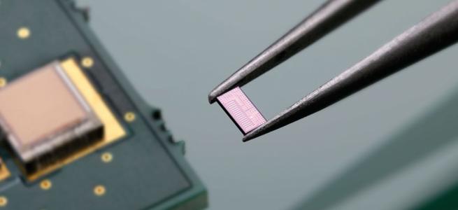
“On the one hand, our massively time-interleaved slope-ADC design exploits the paradigm that slow-speed, but extremely small channels make for a more efficient conversion per area. Secondly, by arranging (lots of) these channels in a two-dimensional array, the length of the interconnection lines is minimized, and the power dissipated through parasitics is reduced. As a result, higher power efficiency and scalability can be achieved, while significantly reducing the ADC’s surface area,” said Joris Van Driessche, program manager at imec. Proof-of-concept: a 42GS/s 7b 16nm massively time-interleaved slope-ADC prototype chip.
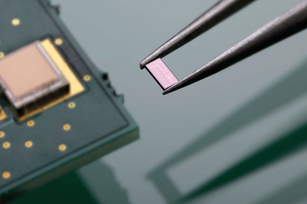
At ISSCC, imec presented a proof-of-concept of its new ADC architecture in the form of a 42GS/s 7b massively time-interleaved slope-ADC prototype chip.
“Even at the relatively modest speed of 42GS/s, the benefits of our approach are clear. Implemented in 16nm FinFET technology, our prototype chip contains an array of 768 slope-ADCs – with a core active area of just 0.07mm². This is at least a factor of two smaller than conventional approaches. It also has a state-of-the-art power consumption of 96mW,” commented Joris Van Driessche. “In other words, this is the first proof that our novel architecture works. And its benefits will only become more significant as we move to higher speeds (150GS/s and beyond).”
In fact, a 5nm ADC using the same architecture is currently being completed – targeting sampling rates well above 150GS/s while achieving extremely low power consumption. In parallel, the team has started exploring a 2nm implementation, targeting speeds in excess of 250GS/s.
“We believe this is an important stepping stone in the development of a whole new generation of small-area, low-power ADCs to support tomorrow’s wireline applications. It overcomes the limitations of SAR ADC implementations, which risk running out of steam when required to operate at extremely high speeds,” concluded Van Driessche.
Imec is inviting additional partners to join this research effort – such as fabless companies specializing in the development of wireline connectivity building blocks. Moreover, licensing options are available for those companies seeking access to imec’s ADC IP blocks.
Imec has a long track record in developing high-speed integrated circuits for photonics applications. One of its research tracks is aimed at creating optical transceivers (and their various building blocks) that can keep up with the exploding data rates of wireline applications. Late last year, for example, imec researchers at Ghent University developed an optical receiver achieving a gross data rate of 200 Gbps by co-integrating a traveling-wave SiGe BiCMOS transimpedance amplifier with a silicon photonics Ge photodetector to combine the need for speed with a scalable and affordable implementation. The pursuit of a new generation of ADCs and DACs clearly complements this research effort, taking ADC development to a whole new level.
Compact wireless powering technology
Imec’s ultrasound-based proof-of-concept for wireless powering of implantable devices is a solution of just 8 mm x 5.3 mm enableing precise beam steering (up to a 53-degree angle) and requires 69 percent less power consumption – believed to make it the smallest, lowest power consuming, wireless ultrasound powering unit among state-of-the-art systems. The cutting-edge concept of global charge-redistribution adiabatic driver addresses challenges associated with traditional tethered connections or batteries and paves the way for minimally invasive, wireless (neural) implants.
The need for wireless powering
Intracortical neural recordings, key for understanding and treating neurological disorders, face challenges in their powering. Traditional invasive wiring risks complications such as scarring and infection, while battery integration (removing the necessity for tethering) brings size and chemical leak concerns.
The use of global charge-redistribution adiabatic drive: a paradigm shift
Eliminating the need for invasive procedures or bulky components, imec and Delft University of Technology have designed ultrasound technology that wirelessly delivers power to neural implants, successfully traversing distances from the skull to the brain’s cortex, within the ERC-funded “Intranet of Neurons” project.
To realize this, the researchers introduced a unique adiabatic driving technique based on the concept of “global charge redistribution” (GCR). Unlike traditional adiabatic driving methods, this approach leverages the parasitic capacitors of the ultrasound transducer array itself and recycles charges. This eliminates the need for external capacitors to redistribute charges and allows for a more compact design. The chip, fabricated in 65nm CMOS, features a fully integrated 116μm×116μm driving unit that allows for 69 percent power savings compared to conventional class-D driving. This design makes it both the smallest ultrasonic adiabatic driving unit with the lowest power consumption among state-of-the-art systems.
For in vivo use, beam steering up to large angles (>45˚) is critical to maximize power delivery and compensate for brain micro-movements and misalignments (such as those occurring during surgery and respiration). With the introduction of a beam steering controller, imec’s GCR scheme enables beam steering up to 53 degrees.
“While many neural implant technologies are currently making significant progress in sensing and stimulation, wireless interfaces, as one of the crucial components of implants, still have much room for improvement - particularly in terms of power efficiency and form factor. To bridge this gap and unlock the full potential of neural implants, we are leveraging our unique wireless-, powering-, and telemetry technologies, to develop minimally invasive wireless systems tailored for miniaturized implants, with applications beyond intracortical neural implants”, commented Yao-Hong Liu, Scientific Director at imec. “We aspire to showcase the practical application of our technology in real in vivo conditions, with our ongoing advancements, particularly in areas such as micro-system integration and packaging, and welcome collaborations with medical professionals or researchers.”
The article “An Ultrasound-Powering TX with a Global Charge-Redistribution Adiabatic Drive Achieving 69% Power Reduction and 53° Maximum Beam Steering Angle for Implantable Applications,” provides a detailed overview of the technological advancements, including the proposed architecture, circuit design, and performance metrics. This project Intranet of Neurons has received funding from the European Research Council (ERC) under the European Union’s Horizon 2020 research and innovation program (grant agreement No. 101001448).
Low-power UWB receiver chip
Imec’s low-power ultra-wideband (UWB) receiver chip is said to be ten times more resilient against interference from Wi-Fi and (beyond) 5G signals than existing, state-of-the-art UWB devices. Imec’s breakthrough chip is a major step forward in developing and deploying next-generation UWB applications, which are becoming increasingly safety-critical. Think of child presence detection systems in the automotive sector, where reliability and assured availability are paramount, or manufacturing environments, where UWB’s precise localization capabilities could ensure the safety of human workers operating near robotic arms, AGVs, and other automated machinery.
In the coming months and years, the spectrum allocated for ultra-wideband communications (typically spanning the 6 to 10GHz frequency range) will face increasing competition from other wireless technologies that eye the same frequencies to extend their reach. The recent approval of Wi-Fi 6e, for instance, positions it to operate in the 5.925 to 7.125GHz band. And (beyond) 5G technologies are also expanding into the upper 6GHz band – given that their existing frequency ranges risk running out of steam. For the UWB industry, this requires proactive measures, especially as UWB technology moves beyond (traditional) secure keyless entry applications to safety-critical automotive and industrial automation functions. In other words, there is a growing need for solutions that allow UWB and other wireless technologies to coexist seamlessly in the same frequency bands.

Imec’s new IR-UWB receiver: -13dBm blocker resilience, and 7.6mW power consumption. Imec’s new impulse radio (IR) UWB receiver chip – implemented in a 22nm FDSOI process, and with a compact active area of 0.32mm² – stands out as a pioneering solution to avoid interference between UWB and other wireless signals.
To enhance the receiver’s blocking performance, a transformer-coupled bandpass filter (BPF) is integrated into the complementary common gate (CCG) stage of the UWB low-noise amplifier (LNA) front-end. As such, imec’s receiver exhibits an exceptional -13dBm blocker resilience, making it ten times more resilient against Wi-Fi and (beyond) 5G interference compared to existing solutions.
Moreover, several circuit design optimizations enable the receiver to achieve its outstanding interference resilience at the lowest power consumption (7.6mW). This efficiency allows the receiver analog front-end (AFE) to operate ten times longer on the same (battery) power compared to current IEEE 802.15.4a/z compatible UWB devices, and twice as long as described in recent research papers. The use of bandpass filters is a widely accepted method for dealing with unwanted signals, such as Wi-Fi, before they enter the receiver. However, imec’s patented implementation to reduce intermodulation distortion significantly increases the receiver’s robustness at low power and low supply design.
“To foster its industrial adoption, our UWB receiver not only complies with the existing IEEE 802.15.4z standard; it is also ready to support the upcoming IEEE.802.15.4ab standard. We believe this research, and the underlying collaboration in high-impact industrial ecosystems, are critical steps to enable future wireless technologies to coexist seamlessly across various use cases,” said Christian Bachmann, program director of wireless sensing at imec.
Imec works with industrial partners across the UWB ecosystem through R&D partnerships and IP licensing. Looking ahead, imec is committed to remain at the forefront of UWB innovation. imec invites companies to join its UWB R&D program and extensive partner network.