Enabling the future with next generation power devices

KAZUHIRO UEDA, PRODUCT PLANNER OF WAFER TEST SOLUTIONS AT KEYSIGHT TECHNOLOGIES JAPAN, explains the importance and increasing needs of parametric tests and the test challenges for high-voltage parametric tests as next-generation power devices are developed to meet a growing quantity and variety of applications in the automotive industry and beyond
These are designed to enable automated measurement with high accuracy, speed, and efficiency while switching the measurement resources using a switching matrix (SWM). Typically, a parametric tester is equipped with a source measure unit (SMU) for current-voltage (IV) characteristics, ensuring precision in sub-pA low current measurements. In addition, it usually features an LCR meter for capacitance-voltage (CV) measurement, a pulse generator, a digital volt meter (DVM), and much more.
Parametric test challenges for high voltage power devices
While the need for parametric testing is essential in order to improve device reliability and yield, there are several challenges when it comes to performing the parametric test with high-volage devices that don’t appear in low-volage testing.
The first challenge is that most parametric testers are in fact designed for low-voltage device testing. Therefore the voltage range is limited to several hundred volts, and it cannot cover high-voltage device testing requirements. One possible solution is using an existing high-voltage test system such as a chip tester in combination with the low-voltage parametric tester to complement the missing high-voltage coverage. However, such high-voltage test systems are not designed for parametric tests, so the low current measurement performance, measurement accuracy, measurement flexibility and connectivity are not optimised for parametric tests for TEG. In addition, the combination of a low-voltage tester and high-voltage tester would be costly when it comes to both test efficiency and footprint.

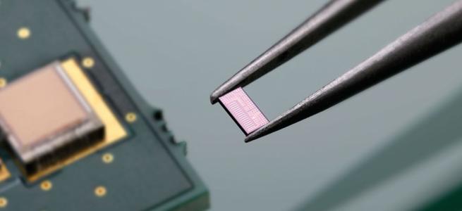
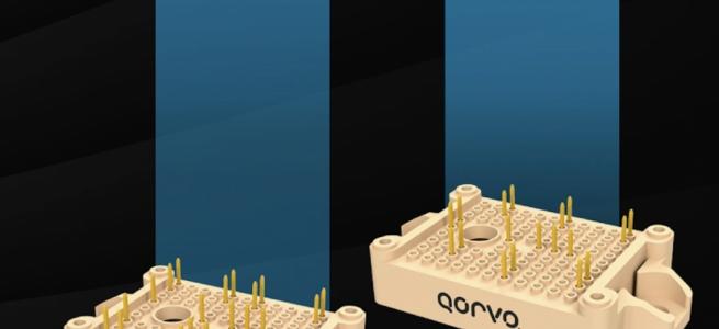
Figure 1.3kV HV-Switching Matrix (HV-SWM).
A second idea explored is using a special parametric tester designed to cover both high-voltage and low-voltage measurements. However, usually high-voltage parametric testers have some limitations when it comes to the number of high-voltage applicable pins and the flexibility of connections due to the technical difficulties of high-voltage relays and switches.
In addition, typical high-voltage parametric testers don’t have sufficient voltage coverage for next-generation power devices exceeding 1kV or more. This means that the device under test needs to be changed, such as changing the probe cards to test all desired devices leading to additional effort and test time.
Wafer manufacturers also need to pay attention to operator safety, and they need to ensure they have the right protected equipment to safeguard against hazardous voltage and other areas of concern when it comes to high-voltage testing. For example, compressed dry air (CDA) would need to be used with a high-voltage probe card to suppress arc/discharge at the probe pin tips.
From a facility management perspective, wafer manufacturers will need to ensure safety regulations are met and in compliance with SEMI S2 for a test system. Considering the automotive space as an example, the test system would be required to meet the general requirements for the competence of testing and calibration laboratories to satisfy the requirements of the International Automotive Task Force (ISO-17025).
There is no comprehensive solution in the market that can meet the increasing needs of parametric tests for high-voltage devices. Thus, power device manufacturers are facing the challenges of test limitation, test cost, test time, and safety and regulatory requirements.

Figure 2. The measurement example as a result of a high-voltage MOSFET
(Vdss spec = 2500V) using Keysight’s new high-voltage parametric tester.
The breakthrough solution for high voltage parametric test up to 3kV
To overcome the challenges posed by high voltage parametric testing, a new type of parametric tester with a switching matrix (SWM) tolerant beyond 1kV is needed. One of the key solutions is to develop a switching matrix that can support both high-voltage and low current in one pass test.
The use of newly designed high-voltage relays allow 3kV switching while meeting the isolation and safety requirements to comply with the safety requirements for electrical equipment for measurement, control, and laboratory use (IEC61010). The new high-voltage relay also provides active guarding to enable sub-pA current measurement by preventing leakage current.
As shown in Figure 1, the low leakage protection circuits are built in to protect and prevent the low-voltage measurement sections from damage due to misconnection even for a 3kV measurement environment. The system is equipped with so many unique and breakthrough technologies to make itself the only choice for high-voltage parametric tests. The new high-voltage parametric tester integrates new HV-SWM up to 30 pins including a chuck terminal with high-voltage SMU(HVSMU) up to 3kV and low-voltage SMU (LVSMU) proven by de-facto standard B1505A power device analyser in SiC/GaN research and development. In addition, capacitance measurement up to 1kV, pulsed measurement and traditional measurement can be performed by other instruments used in low-voltage parametric tester. This system is also designed to meet regulatory needs such as safety regulations, SEMI S2 compliance and ISO17025 certificate. This system can integrate with a wafer prober and probe card to perform high-voltage testing as a total system.
These comprehensive measurement capabilities will enable manufacturers to perform various measurements across different devices more accurately and with flexibly.
In this measurement, the voltage is swept from low-voltage (0V) to high-voltage (3kV) seamlessly. Measurement captures the Idss characteristics (Vds-Id) from pA range low current and rapid current increase by breakdown around 2900V.
As shown, low-voltage device characteristics can also be measured accurately as well as conventional low-voltage parametric tester up to 1A. As of early 2024, the new high-voltage parametric tester is being jointly evaluated by multiple power semiconductor leaders.

Figure 3. The measurement result of output characteristics (Vce-Ic) of transistor (IGBT).
Looking ahead
Carbon neutrality and the move toward zero emissions continue to be the next-generation challenge across all industries as we look to mitigate the effects of global climate change. As shown in the EV/HEC space we are starting to see strong strides being made.
As we look ahead, the innovation of power semiconductor technologies and next-generation power devices such as SiC/GaN are expected to be a key solution, and will enable the industry to move from research and development to production on a mass scale. With this in mind, the importance and increasing needs of parametric tests and the test challenges for high-voltage parametric tests should not be overlooked.