Enhancing β-Ga₂O₃ diodes with oxygen annealing
Oxygen annealing and self-aligned mesa-termination takes β-Ga2O3 diodes further down the pathway to commercialisation.
While β-Ga2O3 power electronics has come a long way, challenges remain, including establishing high-yield processes for producing large-area devices with adequate breakdown voltages.
Making recent substantial progress on that particular front is a partnership between researchers at the University of Science and Technology of China and Hebei Semiconductor Research Institute. This team has shown that oxygen annealing of samples produced by HVPE of β-Ga2O3 reduces the surface roughness and the dislocation density of these films, leading to an increase in the breakdown voltage of Schottky barrier diodes.
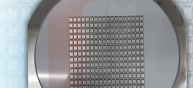
According to team spokesman Feihong Wu, another of this team’s breakthroughs is the use of mesa termination, which alongside the oxygen annealing has been used in the fabrication of devices as large as 3 mm by 3 mm. These Schottky barrier diodes, capable of blocking more than 700 V, deliver 8.7 A under a forward bias of 2 V.
Many techniques are available for the epitaxial growth of β-Ga2O3, including HVPE, MOCVD and MBE. Of these, MOCVD produces superior mobilities, while HVPE is renowned for the rapid growth of thick films and relatively low equipment costs.
Wu points out that the commercially available β-Ga2O3 samples sold by Novel Crystal Technology, Japan, are produced by HVPE.
“Therefore, it can be acknowledged that HVPE currently holds certain advantages,” says Wu. “However, since commercially viable β-Ga2O3 samples are still under development, it is premature to determine which method is superior.
To investigate the influence of oxygen annealing, Wu and co-workers produced a portfolio of devices with undisclosed dimensions – but significantly smaller than 3 mm by 3 mm – using epiwafers from Novel Crystal Technology that feature a 10 μm-thick lightly silicon-doped drift layer, deposited by HVPE on a tin-doped β-Ga2O3 substrate with a carrier concentration of 5 x 1018 cm-3.
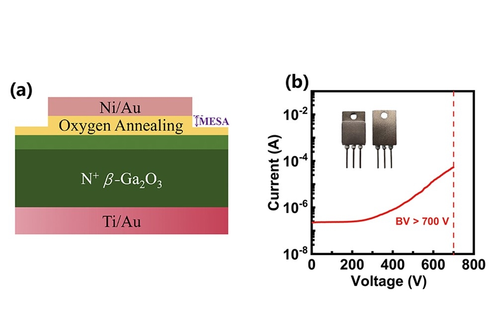
Fabrication of the Schottky barrier diodes began by chemical cleaning, followed by thermal annealing for 30 minutes at either 200 °C, 400 °C, 600 °C or 800 °C. To eliminate the increase in ohmic contact resistance that results from annealing, the team turned to inductively coupled plasma etching, before adding contacts and then defining mesas with inductively coupled plasma etching (see Figure).
According to atomic force microscopy, annealing reduces the root-mean-square roughness, falling from 0.435 nm to 0.245 nm for a 2 µm by 2 µm scan area.
The current density of the team’s diodes under a forward bias of 2 V falls with higher annealing temperatures, due to decreases in carrier concentration. The Schottky barrier height peaks at 1.16 eV, for annealing at 600 °C, and the breakdown voltage peaks at 400 °C. Wu and colleagues have also considered the power figure-of-merit, which peaks at 173 MW cm-2 at 400 °C, declared to be the optimum annealing temperature.
Etching, employed to produce the mesa structures, leads to increases in blocking voltage for all annealing temperatures, and is attributed to more extensive repairing of surface defects.
The team packaged its 3 mm by 3 mm diode in a TO-254 shell, using a parallel sealing and welding process to protect the device in a nitrogen environment. Benchmarking this device revealed that its power-figure-of-merit of 45 MW cm-2 is at the forefront of reported work.
Wu says that many of the devices used for benchmarking differ from their diode by employing complex terminal structures. “While there are some devices of similar area with simple structures, their performance does not match that of our device.”
One of the team’s plans is to develop a deeper understanding of the repair mechanism provided by oxidation annealing.
“Additionally, we aim to investigate the effects of oxygen annealing on mesa termination,” says Wu. “For instance, we seek to understand why the device breakdown voltage experiences a significant increase when thermal oxidation is combined with mesa termination.”
Pictured above: (a) The addition of a mesa helps increase the blocking voltage (b) of β-Ga2O3 Schottky barrier diodes.
Reference
F. Wu et al. Appl. Phys Express 17 036504 (2024)