
NXP and Arizona State University to work on GaN packaging
$17.5 million investment deepens relationship between ASU and NXP
A new partnership with NXP Semiconductors focused on packaging, is the latest development in Arizona State University (ASU) finding new ways to advance Arizona’s expanding semiconductor manufacturing industry.
With support from Arizona Commerce Authority and in partnership with NXP, ASU has received a $17.5 million investment to expand and enhance Arizona’s fan-out, wafer-level packaging R&D and workforce training capabilities, and drive the creation of a GaN manufacturing and research ecosystem.
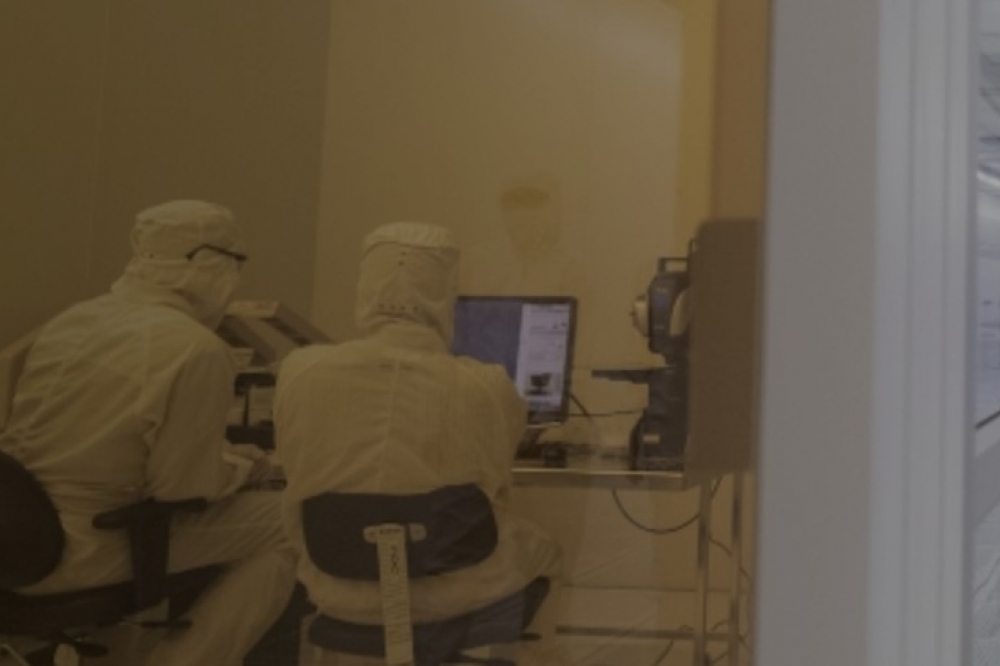
ASU will use the funding to purchase equipment to enhance the capabilities of ASU’s MacroTechnology Works in Tempe. The university plans to expand advanced packaging and GaN research to additional capabilities that support 6G, the Internet of Things, machine learning and more.
The expansion will also include student opportunities and workforce development initiatives such as internships and university joint research, and next-gen GaN research development for 6G in partnership with NXP in Chandler.
The state investment goes along with federal investment through the CHIPS and Science Act and significant private sector investment in ASU to enable the university to continue its mission to drive research innovation and the education of the wokers who will fill the jobs that are being created.
Already working in partnership, the agreement deepens the relationship between ASU and NXP. “We are excited for the opportunity to collaborate with ASU, helping train and develop the engineers of the future, who could one day contribute to the development of critical communications infrastructure benefitting both the state of Arizona and U.S. as a whole,” said Jim Norling, vice president of product management, radio power, at NXP Semiconductors. “This partnership will drive innovation in 6G, taking lab concepts through joint research to full-scale manufacturing.”
The expanded capabilities at MacroTechnology Works in Tempe will support future growth opportunities within Arizona’s semiconductor ecosystem. The ASU expansion also builds on Arizona’s efforts to establish shared semiconductor research and manufacturing facilities that postion the state for additional federal investments through the CHIPS program.
“The partnership will contribute not only to the educational journey of our students, which is our core mission, but also to the success of semiconductor industry leaders and startup companies in Arizona,” said Sally Morton, executive vice president of ASU’s Knowledge Enterprise. “Packaging is the final step in the manufacturing process and it is where some of the greatest innovation comes as we look to increase the capacity and speed of semiconductor chips.”


