
New contacts enhance heteroepitaxial Ga2O3 MOSFETs
Ga2O3-on-sapphire MOSFETs raise the bar for the breakdown voltage
Researchers from South Korea are claiming to have broken new ground for the breakdown voltage of heteroepitaxial Ga2O3 MOSFETs. The transistors made by the team from Soongsil University, Korea Institute of Ceramic Engineering and Technology and the Korea Electrotechnology Research Institute are capable of blocking up to 2.3 kV.
The team attributes the record-breaking breakdown voltages of its MOSFETs to a new metal stack for the source and drain electrodes – it is Ti/Al/Ni/Au.
Team spokesman Geonwook Yoo from Soongsil University told Compound Semiconductor that in addition to the new metal stack, the record breakdown voltage may result from the relatively high temperature used to form the HfO2 gate dielectric. “It successfully reduces not only a surface leakage path, but also a scattering effect induced from the rough silicon-doped a-Ga2O3 layer.”
The a-Ga2O3 MOSFETs are formed on sapphire. It is argued that by avoiding a native substrate, the MOSFETs are not impaired by the poor thermal conductivity of this foundation. The switch to c-plane sapphire improves thermal management through superior thermal conductivity, while providing a platform that only has small differences in the thermal coefficient and lattice constant compared with Ga2O3.
Production of the a-Ga2O3 MOSFETs involved HVPE, a growth technique that offers many merits for high-volume production, including rapid deposition at a relatively low temperature.
Yoo and co-workers produced their devices by loading 2-inch (0001) sapphire into a HVPE chamber, heating this to 470 °C, and growing 0.9 µm of undoped a-Ga2O3 followed by 0.3 µm of silicon-doped a-Ga2O3 in just 10 minutes. Fabrication of the transistors involved: reactive-ion etching to form mesa structures about 500 nm-thick; the introduction of source and drain electrodes by electron-beam evaporation, patterning, lift-off and rapid thermal annealing; and the addition, by atomic layer deposition, of a 20 nm-thick HfO2 gate dielectric that is capped with a Ni/Au stack. The team also produced a control with conventional Ti/Au source and drain electrodes.
According to atomic force microscopy scans of the source and drain electrodes, the new stack is far rougher than its conventional counterpart, with the value for root-mean-square roughness increasing from around 1.1 nm to 11 nm. This is attributed to Ni-Al alloy aggregation during the rapid thermal anneal.
Using transmission-line measurements, the team extracted values for the contact resistance. Switching the electrode from Ti/Au to Ti/Al/Ni/Au slashed the contact resistance from 1.9 kΩ mm to just 0.2 kΩ mm.
The low contact resistance, which even occurs for a-Ga2O3 layers with a low silicon doping level, results from diffusion of aluminium into the titanium layer during rapid thermal annealing. The resulting Ti-Al inter-metallic phase leads to the generation of many oxygen vacancies at the interface between a-Ga2O3and the inter-metallic compounds.
Electrical measurements on the team’s MOSFETs showed that the new gate stack leads to a significantly higher on current. For both types of device, off current is limited by leakage through the undoped a-Ga2O3 layer, rather than leakage through the gate oxide. The MOSFET with the new gate stack has a field effect mobility of 20.4 cm2 V-1 s-1, which is claimed to be a record for heteroepitaxial Ga2O3 MOSFETs.
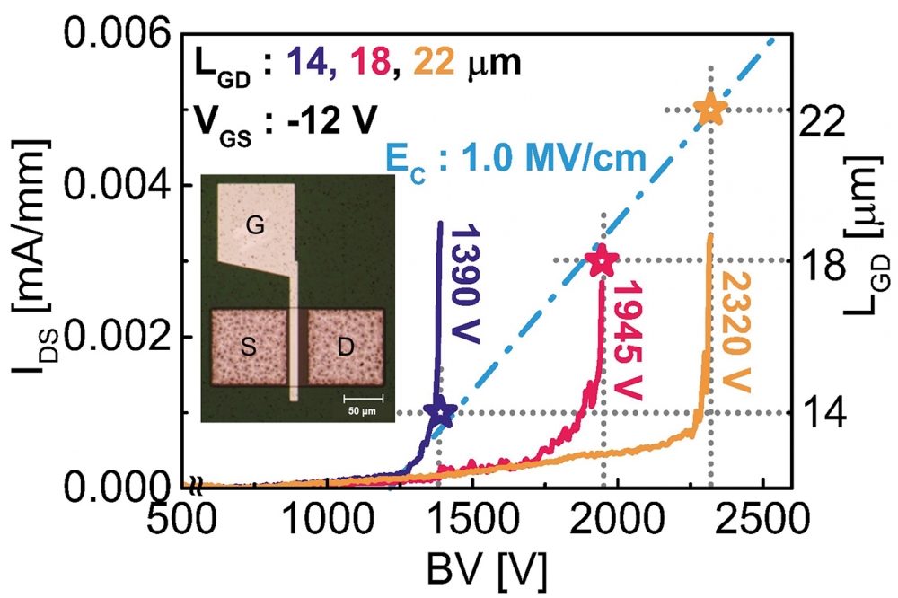
Yoo and co-workers have also conducted three-terminal off-state breakdown voltage measurements, investigating MOSFETs with gate-to-drain distances of 22 µm, 18 µm and 14 µm. They found that the breakdown voltage increases with distance to hit 2320 V, indicating a critical field of 1 MV cm-1.
One of the plans for the team is to continue to develop hetero-epitaxial growth technology for substrate diameters of 6-inch or more. Another aim is to advance MOSFET design, introducing the likes of a field plate and a passivation layer. These refinements should boost the blocking voltage and enhance the figure-of-merit for power.
Ref: Y. J. Jeong et al. Appl. Phys. Express 15 074001 (2022)
Picture caption: Increasing the gate-to-drain distance of the a-Ga2O3 MOSFET increases its breakdown voltage. The inset shows an optical microscopy image of the Ti/Al/Ni/Au metal gate stack.


