
Scientists deposit gallium oxide on 6-inch wafer using HVPE
Japanese project overcomes high cost of epitaxial deposition of β-Ga2O3
As part of NEDO's 'Strategic Energy Conservation Technology Innovation Program', Novel Crystal Technology, in collaboration with Taiyo Nippon Sanso, and Tokyo University of Agriculture and Technology, have for the first time deposited β-Ga2O3, a next-generation semiconductor material, on a 6-inch test wafer with halide vapour phase epitaxy (HVPE) .
Widespread adoption of β-Ga2O3 power devices is expected to lead to energy savings for inverters used in industrial machinery, residential photovoltaic power generation systems, and next-generation EVs. The partners think their recent achievement will overcome the issue of the high cost of epitaxial deposition of β-Ga2O3 and lead to epitaxial deposition equipment capable of mass-producing large-diameter and epitaxial wafers.
Unlike SiC and GaN wafers, β-Ga2O3 wafers can be manufactured in the melt growth method in which bulk crystals grow quickly and it is easy to obtain a large-diameter wafer. However, while the HVPE method has a low raw-material cost and provides a high-purity deposition, current equipment can make only small diameter (2 inches or 4 inches) single wafers. This problem means there is great demand for equipment capable of mass-producing large-diameter (6 inch or 8 inch) wafers in batches in order to reduce the epitaxial deposition cost involved in the HVPE method.
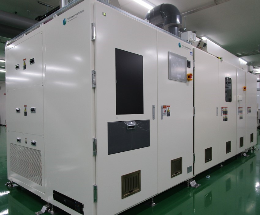
Novel Crystal Technology and Taiyo Nippon Sanso and Tokyo University of Agriculture and Technology have been developing the epitaxial deposition equipment for mass-producing large-diameter β-Ga2O3 wafers. In particular, they have developed external supply technology for the metal chloride that is the raw material of the HVPE method during the 'incubation' research and development phase of this program in FY2019. The partners set up 6-inch single-wafer HVPE equipment and evaluated it to establish the basic technology of mass production in the practical development phase in FY2020-2021.(Pictured above is the 6-inch single-wafer HVPE equipment the partners developed).
In addition to depositing β-Ga2O3 on a 6-inch test wafer (with a sapphire substrate), they achieved a film thickness distribution of ± 10 percent or less. Furthermore, they confirmed that uniform epitaxial deposition is possible by optimising the epitaxial deposition conditions and using a unique raw-material nozzle structure. They believe these achievements will greatly advance the development of the large-diameter-wafer batch-type mass-production equipment. It is estimated that the energy saving effect of the β-Ga2O3 epitaxial deposition process and mass adoption of devices will be about 210,000 kL/year by 2030.
Taiyo Nippon Sanso, Tokyo University of Agriculture and Technology and Novel Crystal Technology will continue to develop mass-production equipment for β-Ga2O3 epitaxial deposition in the NEDO project and perform epitaxial film deposition using 6-inch β-Ga2O3 wafers and β-Ga2O3 thin film.
The aims is to develop high-quality β-Ga2O3 epitaxial deposition technology by evaluating the electrical characteristics and defects existing in the film and aim to commercialise the equipment in 2024.
β-Ga2O3 epitaxial wafers manufactured by the HVPE method are mainly used for SBDs and FETs, and the market is expected to grow to about 59 billion yen by 2030. By entering the market with this mass-production equipment and popularizing β-Ga2O3 power devices, the partners bope to provide energy savings for next-generation EVs and other power applications.


